Carregar apresentação
A apresentação está carregando. Por favor, espere

1
Resumo anterior Modulação
Eletromecânica – chopper Eletro-óptica Efeito Pockel Efeito Kerr Magneto-óptica Efeito Faraday Magneto-Kerr Acusto-óptica Reflexão de Bragg, célula de Bragg Xstal de quartzo, PZT Fotolitografia. Demo de materias p/ fotolitografia: placa cobreadas de fenolite, fibra de vidro, face simples , face duplas. Fotolito. Litografia

2
Eletro-óptico Pockel e Kerr

3
Magnetooptical Kerr Effect = MOKE

4
O passo a passo da litografia
Ver em: e procurar por Basic Lithography Tutorial é um java script com animação.

5
SPM lithography

8
A colocação de água aumenta a NA (nsenq)
Litografia de imersão Limite de resolução para litografia é usando a eq de Rayleigh: W é a largura da linha impressa. Onde k1 é o fator de resolução, l é o comprimento de onda da radiação de exposição e NA é a apertura numérica. Immersion lithography Stepper resolution is normally expressed as W = R = k (process coefficient) x lambda (light source wavelength) / NA (numerical aperture; the brightness of the projection lens). The shorter the wavelength of the light source and the higher the NA of the lens, the higher the resulting resolution. NA itself is expressed as n x sin theta, where n is the refractive index of the material through which the light passes, and theta is the angle of incidence of that light. Normally this light beam passes through air, meaning that n = 1. In immersion lithography, however, a liquid with a refractive index of greater than 1 is placed between the projection lens and the wafer, resulting in a corresponding increase in the NA of the system. For a given incident angle theta, minimum feature size can be reduced (improved) to 1/n. For a given NA theta can be reduced, allowing the focal depth to be increased n times. If an ArF laser is used as the light source, distilled water with a refractive index of 1.44 is placed between the projection lens and the wafer. This technique has been used for some time in microscopes. A colocação de água aumenta a NA (nsenq)
 x lambda (light source wavelength) / NA (numerical aperture; the brightness of the projection lens). The shorter the wavelength of the light source and the higher the NA of the lens, the higher the resulting resolution. NA itself is expressed as n x sin theta, where n is the refractive index of the material through which the light passes, and theta is the angle of incidence of that light. Normally this light beam passes through air, meaning that n = 1. In immersion lithography, however, a liquid with a refractive index of greater than 1 is placed between the projection lens and the wafer, resulting in a corresponding increase in the NA of the system. For a given incident angle theta, minimum feature size can be reduced (improved) to 1/n. For a given NA theta can be reduced, allowing the focal depth to be increased n times. If an ArF laser is used as the light source, distilled water with a refractive index of 1.44 is placed between the projection lens and the wafer. This technique has been used for some time in microscopes. A colocação de água aumenta a NA (nsenq)")
9
Litografia de imersão The most recent SEMATECH-led Litho Forum, an invite only event for around 100 of the top lithography experts in the semiconductor industry are reported to have confirmed that they expect 193nm ArF immersion lithography to pattern critical layers at the 45nm half-pitch node in 2009 as well as continue at the 32nm half-pitch "The surveys indicated an aggressive adherence to the half-pitch targets identified by the International Technology Roadmap for Semiconductors (ITRS)," said Michael Lercel, SEMATECH Lithography director and conference chair. "However, cost concerns for new approaches are in the forefront of many people's minds." Immersion lithography is a technology in which lithographic exposure of a resist coated wafer is performed with purified water introduced between the projection lens of a stepper and the wafer. The light source of the leading-edge stepper currently used in production lines is the ArF 193nm excimer laser, and the resolution is approximately 90nm. 65nm is said to be the limit even for a system for research and development. The idea behind immersion lithography is to use the same ArF light source and yet realize a semiconductor process technology that achieves a resolution higher than 65nm. ================================================================================================= This is in respect to double patterning that could be necessary at the 32nm node should EUV Lithography not be ready for volume production in that time frame. EUVL was deemed the only choice at the 22nm node as concerns have arisen over the extendibility of immersion to higher NA's that will require higher index fluids and lenses. Although other technologies such as maskless lithography and nano-imprinting technology were reviewed at the forum, it would seem that optical lithography will continue to be the preferred choice through to the 22nm node.
, said Michael Lercel, SEMATECH Lithography director and conference chair. However, cost concerns for new approaches are in the forefront of many people s minds. Immersion lithography is a technology in which lithographic exposure of a resist coated wafer is performed with purified water introduced between the projection lens of a stepper and the wafer. The light source of the leading-edge stepper currently used in production lines is the ArF 193nm excimer laser, and the resolution is approximately 90nm. 65nm is said to be the limit even for a system for research and development. The idea behind immersion lithography is to use the same ArF light source and yet realize a semiconductor process technology that achieves a resolution higher than 65nm. ================================================================================================= This is in respect to double patterning that could be necessary at the 32nm node should EUV Lithography not be ready for volume production in that time frame. EUVL was deemed the only choice at the 22nm node as concerns have arisen over the extendibility of immersion to higher NA s that will require higher index fluids and lenses. Although other technologies such as maskless lithography and nano-imprinting technology were reviewed at the forum, it would seem that optical lithography will continue to be the preferred choice through to the 22nm node.")
10
Evolução da largura de linha mínima e l
O fator de resolução k1 é um fator complexo que depende de várias variáveis no processo de fotolitografia: qld do fotoresist, técnicas de melhoramento da resolução, tipo de mascaras, tipo de iluminação, entre outros.

11
Evolução de NA e k1 G-line => 436nm I-line => 365nm
Laser de ArF=> 193 nm g-line An emission line of the mercury discharge lamp centered about 436nm. In the visible portion of the EM spectrum. First generation of lithography tools used this emission line for photoresist exposure. Yields resolution of 1um in resist. See Description of Rayleigh equation for discussion on resolution dependence on wavelength. i-line An emission line of the mercury discharge lamp centered about 365nm. Second generation of lithography tools used this emission line for photoresist exposure. In the ultraviolet portion of the EM spectrum. Yields resolution of 0.5um in resist. See Description of Rayleigh equation for discussion on resolution dependence on wavelength.

12
Imersão numerical aperture
the product of the lowest index of refraction in the object space multiplied by the sine of half the angular aperture of the objective. numerical aperture (NA) For a microscope, (the half angle of the cone of light accepted by the objective lens) x (refractive index of the medium between the specimen and the lens). Also similarly for the cone of light emerging from the condenser lens. The numerical aperture of a lens system (objective or condenser). It is the sine of one-half the angular aperture times the refractive index of the medium (1.0 for air, for Cargille immersion oil, etc.) between objective and specimen. The numerical aperture is a measure of the light gathering capacity of the lens system and determines its resolving power and depth of field.
 For a microscope, (the half angle of the cone of light accepted by the objective lens) x (refractive index of the medium between the specimen and the lens). Also similarly for the cone of light emerging from the condenser lens. The numerical aperture of a lens system (objective or condenser). It is the sine of one-half the angular aperture times the refractive index of the medium (1.0 for air, for Cargille immersion oil, etc.) between objective and specimen. The numerical aperture is a measure of the light gathering capacity of the lens system and determines its resolving power and depth of field.")
13
Existem vários tipos de processos litográficos
Feixe de elétrons EUV SPL Raio-X Mas

20
Nanoimprint Lithography_NIL_seminar_march07_Optical Vs. Soft Vs
Nanoimprint Lithography_NIL_seminar_march07_Optical Vs. Soft Vs. Nanoimprint Lithography.pdf

22
Independente da forma como é realizada....
Observar o produto final objetivo dos efeitos que desejamos

23
Óptica integrada Desenvolvimento de dispositivos ópticos miniaturizados, em escala de micro – nano, de alta funcionalidade sobre substratos. Nesta área é possível distinguir: Circuitos ópticos integrados. A luz é confinada em guias de onda de filmes finos, depositados ou cavados no substrato (vidro, xstal dielétrico, semicondutor). Dispositivos ópticos planares
. Dispositivos ópticos planares.")
24
Canais de guia de onda fio de cobre
As guias de onda são feitas por deposição de material sobre o topo do substrato e posteriormente atacado quimicamente para retirar o resto do material. Pode ser ao contrário tb, Fazendo os sulcos por ataque químico e posteriormente preenchido com material da guia de onda Condições: índice de refração maior na guia do resto do material.

25
Outra guia de onda

26
Guia de onda em LiNbO3 Tiras de Ti depositado no padrão de guia de onda desejado sobre substrato de LiNbO3 puro Aquecimento => difusão Obtenção de guia de onda semicircular 6 Lithium Niobate The substrate is single-crystal lithium niobate, and the waveguides are usually part of the substrate with indiffused titanium. Lithium niobate has relatively low propagation loss in the telecommunications band (-0.2 dB/cm) yet has extremely high linear electrooptic coefficients (it is acentric). It can provide very fast and efficient phase shifters and polarization converters. The most common LiNbO3 waveguide is the Ti-diffused waveguide. lo7 Onto a substrate of LiNb03 (pure crystal), Ti strips are deposited in the desired waveguide pattern. Then the device is heated, and the Ti diffuses into the LiNb03 making a semicircular waveguide. This core is not buried, so care must be taken to keep electrodes on top from absorbing the light. The typical waveguide structure is shown in Fig. 53. Vol. 5, No. 2/February 1988/J. Opt. Soc. Am. B
 yet has extremely high linear electrooptic coefficients (it is acentric). It can provide very fast and efficient phase shifters and polarization converters. The most common LiNbO3 waveguide is the Ti-diffused waveguide. lo7 Onto a substrate of LiNb03 (pure crystal), Ti strips are deposited in the desired waveguide pattern. Then the device is heated, and the Ti diffuses into the LiNb03 making a semicircular waveguide. This core is not buried, so care must be taken to keep electrodes on top from absorbing the light. The typical waveguide structure is shown in Fig. 53. Vol. 5, No. 2/February 1988/J. Opt. Soc. Am. B.")
27
Phase Shifter A mudança de fase vem unicamente do efeito Pockels, campo elétrico provocado através dos dois fios de ouro, que fazem a mudança do índice de refração. Tem sido obtidos moduladores de até 40Gb/s. The phase shift arises solely from the Pockels effect. One simply places two gold lines, around the waveguide (see Fig. 54). The electric field then changes the refractive index. 40 Gb/s modulators have been demonstrated. 6.3 DIGITAL SWITCH One can make a digital 2 x 2 switch in LiNb03 by placing electrodes on the waveguides with the same width in an adiabatic coupler (see Sec 2.10).108W hen no voltage is applied, the coupler acts as a 50/50 coupler, as expected. When a voltage is applied to one waveguide, the switch is in either a bar or cross state, and vice versa with application to the other waveguide. Once sufficient voltage is applied to make the two waveguides no longer identical, a further increase in voltage does not further affect the switching. Such switches have been combined in fabrics to make fully integrated spatial cross connects as large as 16 x 16.'09
. The electric field then changes. the refractive index. 40 Gb/s modulators have been demonstrated. 6.3 DIGITAL SWITCH. One can make a digital 2 x 2 switch in LiNb03 by placing electrodes on the. waveguides with the same width in an adiabatic coupler (see Sec 2.10).108W hen. no voltage is applied, the coupler acts as a 50/50 coupler, as expected. When. a voltage is applied to one waveguide, the switch is in either a bar or cross. state, and vice versa with application to the other waveguide. Once sufficient. voltage is applied to make the two waveguides no longer identical, a further. increase in voltage does not further affect the switching. Such switches have. been combined in fabrics to make fully integrated spatial cross connects as. large as 16 x")
28
SAW = Surface Acoustic Wave
Dispositivos acusto-ópticos são fabricados por processos fotolitográficos Tipicamente consiste de dois conjuntos de transdutores interdigitais. Um transdutor converte a energia do sinal elétrico em energia mecânica ondulatória. O outro transdutor faz o processo reverso. A surface acoustic wave (SAW) is an acoustic wave traveling along the surface of a material having some elasticity, with an amplitude that typically decays exponentially with the depth of the substrate. This kind of wave is commonly used in piezoelectric devices called SAW devices in electronics circuits. SAW devices are employed as filters, oscillators and transformers based on the transduction of acoustic waves. Electronic devices employing the SAW normally utilize one or more interdigital transducers (IDTs) to convert acoustic wave to electrical signal and vice versa utilizing the piezoelectric effect of certain materials (quartz, lithium niobate, lithium tantalate, LGS etc). These devices are fabricated utilizing common processes used in the manufacture of silicon integrated circuits. SAW filters have enjoyed successful application in the booming cellular telephones market and provide significant advantages in performance, cost, and size over other filter technologies (digital signal processors, quartz crystals (bulk wave) , LC-filters, and waveguide filters). Significant research has been done in the last 20 years in the area of surface acoustic wave sensors. Sensor applications include all areas of sensing (such as chemical, optical, thermal, pressure, acceleration, and biological). SAW sensors have seen limited commercial success, but are commonly commercially available for some applications such as touchscreen displays. 6.4 A COUSTOOPTIC FILTER A device that has both optical and acoustic waveguides is the acoustooptic filter in LiNbO3. LiNb03 waveguides have different effective indices for TE- and TM-polarized light. However, by applying an acoustic wave over the waveguide, the periodic nature of the wave can cause the TE and TM lights to be phase-matched at a certain wavelength. Then a diagonal-oriented birefringence becomes significant, causing polarization conversion at that wavelength. One way to couple the acoustic wave to the LiNb03 is to use a surface acoustic waveguide, made up of a thin film of a transparent material such as Si02 or In203-doped SiO2."O So if one makes such an acoustic waveguide over an optical waveguide and launches a traveling acoustic wave with a transducer, the polarization in the optical waveguide will be converted at a certain wavelength. The wavelength response will have large sidelobes, however, without apodization. Apodization can be accomplished by tilting the acoustic waveguide with respect to the optical waveguide. The polarization-converted light is, unfortunately, Doppler-shifted by the acoustic wave. One way to avoid this is to have the shifted light pass through another acoustic wave that is traveling in the opposite direction, in a second stage. Several stages must be used to achieve low crosstalk anyway. One can launch a sum of acoustic frequencies in the waveguide making a series of filters, such as for dropping multiple channels in a WDM system. When there is only acoustic frequency, then light that was polarization converted and Doppler shifted has the opposite Doppler shift if it happens to couple back into the original field. However, with multiple acoustic frequencies, polarization-converted light could be Doppler shifted back into the original field with a different Doppler shift, resulting in intensity beating noise. Figure 55 shows the waveguide layout and filter characteristics of an adddrop made using acoustooptic polarization converters. Figure 1. Acoustic wave devices are manufactured by means of a photolithographic process similar to that used to make ICs. The only difference is that no junction exists in acoustic wave sensors.
 is an acoustic wave traveling along the surface of a material having some elasticity, with an amplitude that typically decays exponentially with the depth of the substrate. This kind of wave is commonly used in piezoelectric devices called SAW devices in electronics circuits. SAW devices are employed as filters, oscillators and transformers based on the transduction of acoustic waves. Electronic devices employing the SAW normally utilize one or more interdigital transducers (IDTs) to convert acoustic wave to electrical signal and vice versa utilizing the piezoelectric effect of certain materials (quartz, lithium niobate, lithium tantalate, LGS etc). These devices are fabricated utilizing common processes used in the manufacture of silicon integrated circuits. SAW filters have enjoyed successful application in the booming cellular telephones market and provide significant advantages in performance, cost, and size over other filter technologies (digital signal processors, quartz crystals (bulk wave) , LC-filters, and waveguide filters). Significant research has been done in the last 20 years in the area of surface acoustic wave sensors. Sensor applications include all areas of sensing (such as chemical, optical, thermal, pressure, acceleration, and biological). SAW sensors have seen limited commercial success, but are commonly commercially available for some applications such as touchscreen displays. 6.4 A COUSTOOPTIC FILTER. A device that has both optical and acoustic waveguides is the acoustooptic. filter in LiNbO3. LiNb03 waveguides have different effective indices for. TE- and TM-polarized light. However, by applying an acoustic wave over. the waveguide, the periodic nature of the wave can cause the TE and TM. lights to be phase-matched at a certain wavelength. Then a diagonal-oriented. birefringence becomes significant, causing polarization conversion at that. wavelength. One way to couple the acoustic wave to the LiNb03 is to use a surface acoustic. waveguide, made up of a thin film of a transparent material such as Si02. or In203-doped SiO2. O So if one makes such an acoustic waveguide over an. optical waveguide and launches a traveling acoustic wave with a transducer, the. polarization in the optical waveguide will be converted at a certain wavelength. The wavelength response will have large sidelobes, however, without apodization. Apodization can be accomplished by tilting the acoustic waveguide with. respect to the optical waveguide. The polarization-converted light is, unfortunately, Doppler-shifted by the. acoustic wave. One way to avoid this is to have the shifted light pass through. another acoustic wave that is traveling in the opposite direction, in a second. stage. Several stages must be used to achieve low crosstalk anyway. One can launch a sum of acoustic frequencies in the waveguide making. a series of filters, such as for dropping multiple channels in a WDM system. When there is only acoustic frequency, then light that was polarization. converted and Doppler shifted has the opposite Doppler shift if it happens. to couple back into the original field. However, with multiple acoustic frequencies, polarization-converted light could be Doppler shifted back into the. original field with a different Doppler shift, resulting in intensity beating noise. Figure 55 shows the waveguide layout and filter characteristics of an adddrop. made using acoustooptic polarization converters. Figure 1. Acoustic wave devices are manufactured by means of a photolithographic process similar to that used to make ICs. The only difference is that no junction exists in acoustic wave sensors.")
29
Diferentes arranjos dos eletrodos
IDT =InterDigital Transducer SOME UNUSUAL PROPERTIES OF SAW DEVICES Question 2: Before we go any further, tell me if surface acoustic wave (SAW) filters are analog or digital devices? Answer 2: Tricky question! My own view is that some configurations (as in the basic bidirectional interdigital transducer (IDT) structure of Figure 1), can be considered to operate as passive HYBRID analog/digital devices! The basic SAW filter sketched in Figure 1 is indeed a passive analog device. It is just a thin metal film structure deposited on top of a piezoelectric crystal substrate, with no power supplies to worry about. However, this is not the complete answer! Now for the digital part. Look at the constituent input/output IDTs. The layout pattern of these input/output thin metal film patterns is designed to provide the desired bandpass filtering function H(f) = Voutput/Vinput as the SAW propagates along the piezoelectric crystal surface. But these bidirectional IDTs may be considered to act as spatially-sampled versions of the corresponding time-evolving Inverse Discrete Fourier Transform (IDFT) h(t). (Remember that there is a unique correspondence between the frequency response H(f) of a filter, and its impulse response h(t). (Simple concepts for digital signal-processing engineers. Not so simple for old analog circuit designers like me !). Because of this, many digital signal processing techniques can be employed in the design of the IDT patterns. Additionally, SAW filters find applications in many digital communications systems. Question 4: Can SAW bandpass filters operate at harmonic frequencies? Answer 4: Yes. They can operate at selected harmonic frequencies, depending on the metalization ratio h = a/b in Figure 2. Rayleigh-wave delay-line filters employing split-electrode IDTs on YZ-lithium niobate have been reported as operating efficiently up to the 11th harmonic. (See: W. R. Smith, "Basics of the SAW interdigital transducer," in J. H. Collins and L. Masotti (eds.) Computer-Aided Design of Surface Acoustic Wave Devices. Elsevier: New York, Also see: W. R. Smith and W. F. Pedler, "Fundamental- and harmonic-frequency circuit model analysis of interdigital transducers with arbitrary metalization ratios and polarity sequences," IEEE Transactions on Microwave Theory and Techniques, vol. MTT-23, pp , November 1975). The IDTs in Figure 2(a) and Figure 2(b) can operate at selected odd-harmonic frequencies, while the IDT structure in Figure 2(c) can operate at selected even and odd harmonics, depending on the metalization ratio.
 filters are analog or digital devices Answer 2: Tricky question! My own view is that some configurations (as in the basic bidirectional interdigital transducer (IDT) structure of Figure 1), can be considered to operate as passive HYBRID analog/digital devices! The basic SAW filter sketched in Figure 1 is indeed a passive analog device. It is just a thin metal film structure deposited on top of a piezoelectric crystal substrate, with no power supplies to worry about. However, this is not the complete answer! Now for the digital part. Look at the constituent input/output IDTs. The layout pattern of these input/output thin metal film patterns is designed to provide the desired bandpass filtering function H(f) = Voutput/Vinput as the SAW propagates along the piezoelectric crystal surface. But these bidirectional IDTs may be considered to act as spatially-sampled versions of the corresponding time-evolving Inverse Discrete Fourier Transform (IDFT) h(t). (Remember that there is a unique correspondence between the frequency response H(f) of a filter, and its impulse response h(t). (Simple concepts for digital signal-processing engineers. Not so simple for old analog circuit designers like me !). Because of this, many digital signal processing techniques can be employed in the design of the IDT patterns. Additionally, SAW filters find applications in many digital communications systems. Question 4: Can SAW bandpass filters operate at harmonic frequencies Answer 4: Yes. They can operate at selected harmonic frequencies, depending on the metalization ratio h = a/b in Figure 2. Rayleigh-wave delay-line filters employing split-electrode IDTs on YZ-lithium niobate have been reported as operating efficiently up to the 11th harmonic. (See: W. R. Smith, Basics of the SAW interdigital transducer, in J. H. Collins and L. Masotti (eds.) Computer-Aided Design of Surface Acoustic Wave Devices. Elsevier: New York, Also see: W. R. Smith and W. F. Pedler, Fundamental- and harmonic-frequency circuit model analysis of interdigital transducers with arbitrary metalization ratios and polarity sequences, IEEE Transactions on Microwave Theory and Techniques, vol. MTT-23, pp , November 1975). The IDTs in Figure 2(a) and Figure 2(b) can operate at selected odd-harmonic frequencies, while the IDT structure in Figure 2(c) can operate at selected even and odd harmonics, depending on the metalization ratio.")
30
SAW http://kmf.pa.msu.edu/Research/resrch01.asp
Probing Disordered Metallic Films With Surface Acoustic Waves Amy Bylsma Engebretson and Brage Golding Department of Physics and Astronomy, Michigan State University A surface acoustic wave (SAW) can be generated and received by interdigital electrodes, or metal fingers, deposited onto a piezoelectric slab. A SAW is a sound wave which travels along the surface of a solid. Its wavelength is determined by the spacing of the fingers. The above SEM micrograph shows aluminum fingers on lithium niobate. The finger spacing of 1.36 micron (about inches) corresponds to the wave oscillating at frequencies near 700 MHz. By placing thin films of disordered metals in the path of the SAW, we can probe the interaction of the waves with the electrons and defects in the metal. At very low temperatures, near absolute zero, atoms that comprise the defects can absorb energy from the waves and move between two nearby positions. We are studying the characteristics of these transitions in order to arrive at a better understanding of the interactions between defects and electrons.
 can be generated and received by interdigital electrodes, or metal fingers, deposited onto a piezoelectric slab. A SAW is a sound wave which travels along the surface of a solid. Its wavelength is determined by the spacing of the fingers. The above SEM micrograph shows aluminum fingers on lithium niobate. The finger spacing of 1.36 micron (about inches) corresponds to the wave oscillating at frequencies near 700 MHz. By placing thin films of disordered metals in the path of the SAW, we can probe the interaction of the waves with the electrons and defects in the metal. At very low temperatures, near absolute zero, atoms that comprise the defects can absorb energy from the waves and move between two nearby positions. We are studying the characteristics of these transitions in order to arrive at a better understanding of the interactions between defects and electrons.")
31
SAW+fibra = demux = dispositivo integrado
Conversor de polarização acusto-óptico The integrated acoustooptical polarization converter is one of the basic building blocks of the acoustooptical device family. The function of the converters is based on a wavelength selective coupling between orthogonally polarized optical waves induced by surface acoustic waves. Such surface acoustic waves (SAW) are a kind of ultrasound waves confined close to the surface of the crystal. The surface acoustic waves induce a periodic distortion for the optical waves resulting in a polarization conversion. An efficient process requires a coherent accumulation of the conversion along the interaction path. Therefore, the phase-matching condition must be fullfilled: The difference of the wave numbers of the optical waves must be compensated by the wave number of the SAW. This requirement leads to the wavelength selectivity of the conversion process. Via the frequency of the SAW the wavelength for optimum conversion can be adjusted. Devices are usually fabricated to operate in the 1.55 µm range for telecommunication applications. Phase-matching is obtained with SAW frequencies around 170 MHz and the tuning slope is given by about 8 nm/MHz. To enhance the efficiency of the polarization conversion surface acoustical waves can be laterally confined in guiding structures as well. For this purpose acoustical waveguides and even complexer structures such as directional couplers are fabricated. Such acoustical guides are formed by a Ti-indiffusion into the cladding regions of the guiding structures. Due to this indiffusion the stiffness of the material and, hence, the acoustical velocity increases yielding the guiding of the SAWs. Practically, acoustooptical polarization converters are most often realized by embedding a Ti-indiffused optical waveguide into an acoustical waveguide which forms one arm of a directional coupler. A SAW wave is excited via a RF-signal applied to the interdigital transducer electrodes. While propagating along the coupler structure the acoustic power is coupled into the adjacent guide with the embedded optical waveguide. A detailed study of such integrated acoustical structures has been performed to determine optimum coupler dimensions. By an appropriate choice of the waveguide dimensions the SAW fullfills exactly one coupling cycle within the structure. The main advantage of such polarization converters with acoustical directional couplers is an improvement of the spectral characteristics of the conversion process: The conversion characteristics of polarization converters with unguided SAWs or with SAWs guided in straight acoustical guides have pronounced sidelobes. Theoretically, these sidelobes should be about -10 dB below the maximum conversion. To apply the acoustooptical devices as spectral filters for instance in WDM transmission systems such sidelobes are not acceptable. The sources for the sidelobes are the abrupt increase and decrease of the acoustooptical interaction at the transducer and absorber, respectively. With a soft increase and decrease the sidelobes can be tremendously reduced. Such a weighted (apodized) coupling is realized using the directional coupler as the acoustical power is continuously coupled into the interaction region and back again. Typical acoustooptical polarization converters are about 20 mm long. The spectral width (full-width at half maximum) is about 2.0 nm. Sidelobe levels are typically reduced to about -20 dB of the maximum conversion using acoustical directional couplers. RF-drive powers for a complete acoustooptical conversion are in the range of 50 mW. The tuning range is determined by the frequency bandwidth of the transducers to excite the SAWs. Typical tuning ranges exceed 150 nm. However, more than 250 nm has been demonstrated. A special unique feature of the acoustooptical polarization converters is their simultaneous multi-wavelength operation capability. By exciting several SAWs of different frequencies in the converter, conversion is obtained at several wavelengths simultaneously, too. Related publications: J. Frangen, H. Herrmann, R. Ricken, H. Seibert, W. Sohler Integrated optical, acoustically tunable wavelength filter Electron. Lett., Vol. 25, pp (1989) H. Herrmann, St. Schmid Integrated acoustooptical mode converters with weighted coupling using surface acoustic wave directional couplers Electron. Lett, Vol. 28, pp (1992) H. Herrmann, U. Rust, K. Schäfer Tapered acoustical directional couplers for integrated acoustooptical mode converters with weighted coupling J. Lightw. Technol., Vol.13, pp (1995) H. Herrmann, H. Mendis Broadly tunable integrated acoustooptical polarization converters in LiNbO3 Proc. 9th European Conference on Integrated Optics (ECIO'99), Torino, April 1999, pp
 are a kind of ultrasound waves confined close to the surface of the crystal. The surface acoustic waves induce a periodic distortion for the optical waves resulting in a polarization conversion. An efficient process requires a coherent accumulation of the conversion along the interaction path. Therefore, the phase-matching condition must be fullfilled: The difference of the wave numbers of the optical waves must be compensated by the wave number of the SAW. This requirement leads to the wavelength selectivity of the conversion process. Via the frequency of the SAW the wavelength for optimum conversion can be adjusted. Devices are usually fabricated to operate in the 1.55 µm range for telecommunication applications. Phase-matching is obtained with SAW frequencies around 170 MHz and the tuning slope is given by about 8 nm/MHz. To enhance the efficiency of the polarization conversion surface acoustical waves can be laterally confined in guiding structures as well. For this purpose acoustical waveguides and even complexer structures such as directional couplers are fabricated. Such acoustical guides are formed by a Ti-indiffusion into the cladding regions of the guiding structures. Due to this indiffusion the stiffness of the material and, hence, the acoustical velocity increases yielding the guiding of the SAWs. Practically, acoustooptical polarization converters are most often realized by embedding a Ti-indiffused optical waveguide into an acoustical waveguide which forms one arm of a directional coupler. A SAW wave is excited via a RF-signal applied to the interdigital transducer electrodes. While propagating along the coupler structure the acoustic power is coupled into the adjacent guide with the embedded optical waveguide. A detailed study of such integrated acoustical structures has been performed to determine optimum coupler dimensions. By an appropriate choice of the waveguide dimensions the SAW fullfills exactly one coupling cycle within the structure. The main advantage of such polarization converters with acoustical directional couplers is an improvement of the spectral characteristics of the conversion process: The conversion characteristics of polarization converters with unguided SAWs or with SAWs guided in straight acoustical guides have pronounced sidelobes. Theoretically, these sidelobes should be about -10 dB below the maximum conversion. To apply the acoustooptical devices as spectral filters for instance in WDM transmission systems such sidelobes are not acceptable. The sources for the sidelobes are the abrupt increase and decrease of the acoustooptical interaction at the transducer and absorber, respectively. With a soft increase and decrease the sidelobes can be tremendously reduced. Such a weighted (apodized) coupling is realized using the directional coupler as the acoustical power is continuously coupled into the interaction region and back again. Typical acoustooptical polarization converters are about 20 mm long. The spectral width (full-width at half maximum) is about 2.0 nm. Sidelobe levels are typically reduced to about -20 dB of the maximum conversion using acoustical directional couplers. RF-drive powers for a complete acoustooptical conversion are in the range of 50 mW. The tuning range is determined by the frequency bandwidth of the transducers to excite the SAWs. Typical tuning ranges exceed 150 nm. However, more than 250 nm has been demonstrated. A special unique feature of the acoustooptical polarization converters is their simultaneous multi-wavelength operation capability. By exciting several SAWs of different frequencies in the converter, conversion is obtained at several wavelengths simultaneously, too. Related publications: J. Frangen, H. Herrmann, R. Ricken, H. Seibert, W. Sohler Integrated optical, acoustically tunable wavelength filter Electron. Lett., Vol. 25, pp (1989) H. Herrmann, St. Schmid Integrated acoustooptical mode converters with weighted coupling using surface acoustic wave directional couplers Electron. Lett, Vol. 28, pp (1992) H. Herrmann, U. Rust, K. Schäfer Tapered acoustical directional couplers for integrated acoustooptical mode converters with weighted coupling J. Lightw. Technol., Vol.13, pp (1995) H. Herrmann, H. Mendis Broadly tunable integrated acoustooptical polarization converters in LiNbO3 Proc. 9th European Conference on Integrated Optics (ECIO 99), Torino, April 1999, pp")
32
Filtros TE e TM Y2O3 = 17nm Al = 100nm
Comprimento = 1,5mm extinção 20dB TM e 0,5dB atenuação TE Troca de Li por H Região H aumenta ne no diminui TE se acopla na região H, extinção 25dB TM atenua 1dB Acoustooptical Devices Integrated TE- and TM-pass polarizers Polarizers are basic building blocks for the integrated acoustooptical devices. Two types of integrated polarizers are required: TE- and TM-pass polarizers. These polarizers are used to suppress one polarization component propagating in an optical waveguide. In conventional optics several types of polarizers are well-known. Integrated polarizers, however, must be compatible with the specific waveguiding structure. TE-pass polarizers The basic structure of a TE-pass polarizer consists of a sandwich layer system on top of the waveguide structure. This layer system is formed of a dielectric layer (yttrium oxide) followed by an absorbing metallic layer (aluminium). TM-polarized radiation is coupled to surface plasmons of the metallic layer resulting in a strong absorption. On the other hand, TE polarized optical waves are not strongly influenced by the layer system. Best performance properties have been obtained with 17 nm thick yttrium oxide layers and 100 nm thick aluminium layers. In 1.5 mm long structures extinctions of the TM-waves exceeding 20 dB have been achieved. The excess loss for the TE-polarized waves could be kept below 0.5 dB. TM-pass polarizers TM-pass polarizers are fabricated using the proton exchange technique in lithium niobate, i.e. lithium ions of the crystal are substituted by hydrogen ions. The extraordinary index of refraction is increased in the proton exchanged regions and the ordinary index is reduced. TM-pass polarizers are realized by using proton exchanged areas beside the Ti-diffused optical waveguides. In this way the extraordinary polarized (TE) waves couple into the exchanged areas whereas ordinary polarized (TM) waves remain in the Ti-diffused optical waveguide. To optimize TM-pass polarizers careful studies were necessary to investigate the profiles of the refractive indices in proton exchanged lithium niobate and to study the geometry of proton exchanged areas. We found that two major effects determine the polarizer performance: the gap between Ti-diffused optical guide and exchanged regions and the shape of the proton exchanged areas. A narrow gap results in a large extinction but also induces strong additional losses for the TM-waves. Therefore, a compromise has to be found. On the other hand the geometry of the outer boundaries determines the extinction ratio. If parts of the TE-waves are reflected at the outer boundaries they can be recaptured into the optical waveguides resulting in a low extinction ratio. With zig-zag shaped outer boundaries the best performance has been achieved. With such optimized polarizers extinction ratios of more than 25 dB for the TE-waves and excess losses of about 1 dB for the TM-polarized waves have been obtained. Related publications: H. Herrmann, P. Müller-Reich, V. Reimann, R. Ricken, H. Seibert, W. Sohler Integrated optical, TE- and TM-pass, acoustically tunable double stage wavelength filter in LiNbO3 Electron. Lett., Vol. 28, pp (1992) F. Tian, Ch. Harizi, H. Herrmann, V. Reimann, R. Ricken, U. Rust, W. Sohler, F. Wehrmann, S. Westenhöfer Polarization independent integrated optical, acoustically tunable double stage wavelength filter in LiNbO3 J. Lightwave Technol., Vol. 12, pp (1994) U. Hempelmann, H. Herrmann, G. Mrozynski, V. Reimann, W. Sohler Integrated optical proton exchanged TM-pass polarizers in LiNbO3: modelling and experimental performance J. Lightwave Technol. , Vol. 13, pp (1995) If this page is displayed without a button frame on the left side, please reload.Last update: H. Herrmann
 followed by an absorbing metallic layer (aluminium). TM-polarized radiation is coupled to surface plasmons of the metallic layer resulting in a strong absorption. On the other hand, TE polarized optical waves are not strongly influenced by the layer system. Best performance properties have been obtained with 17 nm thick yttrium oxide layers and 100 nm thick aluminium layers. In 1.5 mm long structures extinctions of the TM-waves exceeding 20 dB have been achieved. The excess loss for the TE-polarized waves could be kept below 0.5 dB. TM-pass polarizers TM-pass polarizers are fabricated using the proton exchange technique in lithium niobate, i.e. lithium ions of the crystal are substituted by hydrogen ions. The extraordinary index of refraction is increased in the proton exchanged regions and the ordinary index is reduced. TM-pass polarizers are realized by using proton exchanged areas beside the Ti-diffused optical waveguides. In this way the extraordinary polarized (TE) waves couple into the exchanged areas whereas ordinary polarized (TM) waves remain in the Ti-diffused optical waveguide. To optimize TM-pass polarizers careful studies were necessary to investigate the profiles of the refractive indices in proton exchanged lithium niobate and to study the geometry of proton exchanged areas. We found that two major effects determine the polarizer performance: the gap between Ti-diffused optical guide and exchanged regions and the shape of the proton exchanged areas. A narrow gap results in a large extinction but also induces strong additional losses for the TM-waves. Therefore, a compromise has to be found. On the other hand the geometry of the outer boundaries determines the extinction ratio. If parts of the TE-waves are reflected at the outer boundaries they can be recaptured into the optical waveguides resulting in a low extinction ratio. With zig-zag shaped outer boundaries the best performance has been achieved. With such optimized polarizers extinction ratios of more than 25 dB for the TE-waves and excess losses of about 1 dB for the TM-polarized waves have been obtained. Related publications: H. Herrmann, P. Müller-Reich, V. Reimann, R. Ricken, H. Seibert, W. Sohler Integrated optical, TE- and TM-pass, acoustically tunable double stage wavelength filter in LiNbO3 Electron. Lett., Vol. 28, pp (1992) F. Tian, Ch. Harizi, H. Herrmann, V. Reimann, R. Ricken, U. Rust, W. Sohler, F. Wehrmann, S. Westenhöfer Polarization independent integrated optical, acoustically tunable double stage wavelength filter in LiNbO3 J. Lightwave Technol., Vol. 12, pp (1994) U. Hempelmann, H. Herrmann, G. Mrozynski, V. Reimann, W. Sohler Integrated optical proton exchanged TM-pass polarizers in LiNbO3: modelling and experimental performance J. Lightwave Technol. , Vol. 13, pp (1995) If this page is displayed without a button frame on the left side, please reload.Last update: H. Herrmann.")
33
Materiais eletro-ópticos
Table 1. Electro-Optic Materials Material Abbreviation Chemical Formula Transmission Range (mm) Bandwidth (MHz) Index of Refraction no,ne at wavelength (mm) Ammonium dihydrogen phosphate ADP NH4H2PO4 to 500 1.51, 1.47 at 1.06 Potassium dihydrogen phosphate KDP KH2PO4 > 100 1.51, 1.47 at 0.55 Potassium dideuterium phosphate KD*P KD2PO4 to 350 1.49, 1.46 at 1.06 Lithium niobate LN LiNbO3 to 8000 2.23, 2.16 at 1.06 Lithium tantalate — LiTaO3 to 1000 2.14, at 1.00 Cadmium telluride CdTe 2 - 16 no = 2.6 at 10
 Bandwidth (MHz) Index of Refraction no,ne at wavelength (mm) Ammonium dihydrogen phosphate. ADP. NH4H2PO to , 1.47 at Potassium dihydrogen phosphate. KDP. KH2PO > , 1.47 at Potassium dideuterium phosphate. KD*P. KD2PO to , 1.46 at Lithium niobate. LN. LiNbO to , 2.16 at Lithium tantalate. — LiTaO to , at Cadmium telluride. CdTe no = 2.6 at 10.")
34
Table 2. Acousto-Optic Materials Material Chemical formula
Spectral range (mm) Figure of merit M2 ( m2/W) Bandwidth (MHz) Typical drive power (W) Index of Refraction Acoustic Velocity (m/sec) Fused silica/quartz SiO2 1.6 to 20 6 1.46 (634,3 nm) 5900 Gallium arsenide GaAs 104 to 350 1 3.37 (1.15 mm) 5340 Gallium phosphide GaP 45 to 1000 50 3.31 (1.15 mm) 6320 Germanium Ge 840 to 5 4.0 (10.6 mm) 5500 Lead molybdate PbMoO4 to 50 1 - 2 2.26 (633 nm) 3630 Tellurium dioxide TeO2 35 to 300 4200 Lithium niobate L6Nb03 0.5-2 7 > 300 50-100 2.20 (633nm) 6570
 Figure of merit M2 ( m2/W) Bandwidth (MHz) Typical drive power (W) Index of Refraction. Acoustic Velocity (m/sec) Fused silica/quartz. SiO to (634,3 nm) Gallium arsenide. GaAs to (1.15 mm) Gallium phosphide. GaP to (1.15 mm) Germanium. Ge to (10.6 mm) Lead molybdate. PbMoO to (633 nm) Tellurium dioxide. TeO to Lithium niobate. L6Nb > (633nm)")
35
Dispositivos Podem ser fabricados sobre substratos planares usando processos litográficos comuns e tecnologia de filmes finos. Litografia por feixe de elétrons ou por laser Métodos epitaxiais para fabricação de fontes, detectores e circuitos opto-eletrônicos. AsGa, Si, InP ramificação

36
Acoplamentos Acopladores direcionais como ramificadores
por acoplamento de ondas evanescentes entre acopladores adjacentes Acoplador por reflexão de Bragg

37
Interferômetro Mach-Zehnder
Chaveamento Interferômetro Mach-Zehnder Aquecedor (ms) ou onda acústica (piezo) (ms) ou sinal elétrico num dos braços
 ou onda acústica (piezo) (ms) ou sinal elétrico num dos braços.")
38
Outro tipo de chaveamento
Integrated electro-optic Mach-Zehnder switch realized by Zinc in-diffusion D. A. May-Arrioja and P. LiKamWa College of Optics and Photonics, University of Central Florida, Orlando, FL 5th Iberoamerican Meeting on Optics and 8th Latin American Meeting on Optics, Lasers, and Their Applications, edited by A. Marcano O., J. L. Paz, Proc. of SPIE Vol. 5622 (SPIE, Bellingham, WA, 2004) · X/04/$15 · doi: /
 · X/04/$15 · doi: /")
39
MZI com filtro de Bragg

40
Algumas aplicações Filtros MUX/DEMUX Chaveadores
Amplificadores ópticos Acopladores

41
Meta com óptica integrada
O que transferir e como Meta com óptica integrada

42
Materiais

43
Materiais

44
Componentes fotônicos integrados

45
Mais componentes fotônicos

46
Filtro sintonizável com SAW

47
EDFA integrado

48
Outros processos

49
Comparando duas formas de fazer litografia

50
Escrita direta com laser
Spot ~1 - 5um Tightly Focuses, modulated He-Cd or Argon-ion laser scanned across photresists surface Up to 256 phase levels Serial Process Difficult to accurately transfer structure into substrate Direct ablation of polyimide layer on substrate using an excimer laser is also possible Pattern can be transferred to a VHOE by processing in a 4f optical processor. Optics Communications Volume 281, Issue 20, 15 October 2008, Pages Copyright © 2008 Elsevier B.V. All rights reserved. A volume holographic optical element for optical coupling to single-mode fibers Ching-Cherng Sun , a, , Yau-Jen Changa, Shih-Hsin Maa and Tun-Chien Tenga aDepartment of Optics and Photonics, National Central University, No. 300, Jung-Da Road, Chung-Li 320, Taiwan Received 22 January 2007; revised 11 December 2007; accepted 7 July 2008. Available online 6 August 2008. Abstract We propose and demonstrate a volume holographic optical element (VHOE) for signal-mode fiber coupling and the sending of conjugate waves of reference light for the construction of holographic elements. Given the inherent Bragg conditions of the VHOE, the angular tolerances of the conjugate reading light in both the horizontal and vertical directions are studied under different conditions. Keywords: Volume holography; Single-mode fiber coupling; Alignment tolerance; Holographic optical element VHOE(volume holographic optical element)
 for signal-mode fiber coupling and the sending of conjugate waves of reference light for the construction of holographic elements. Given the inherent Bragg conditions of the VHOE, the angular tolerances of the conjugate reading light in both the horizontal and vertical directions are studied under different conditions. Keywords: Volume holography; Single-mode fiber coupling; Alignment tolerance; Holographic optical element. VHOE(volume holographic optical element)")
51
Processo de photoresist para litografia
SCUM = a film or layer of foul or extraneous matter that forms on the surface of a liquid. DESCUM = limpeza de qq resíduo pelicular existente ou melhor: lavagem

52
Recobrimento do photoresist por spinner

53
Método de replicação

54
Fontes de luz em litografia
G-line nm I-line nm KrF Excimer nm ArF Excimer nm EUV < 13nm g-line A light source used in the repeated exposure of a mask pattern in the photolithography process, with the objective of transferring the pattern to the surface of a wafer. Classified as visible light, g-line light has a wavelength of 436nm and is used to resolve patterns of 0.5 microns or larger. Steppers employing this light are called g-line steppers. i-line A light source used in the repeated exposure of a mask pattern in the photolithography process, with the objective of transferring the pattern to the surface of a wafer. Classified as ultraviolet light, i-line light has a wavelength of 365nm and is used to resolve patterns of 0.25 to 0.5 microns. Steppers employing this light are called i-line steppers.

55
Materiais Fotônicos

56
Materiais Fotônicos Dispositivos Fotônicos Cristais Fotônicos
Algumas referencias Cid Araujo, Óptica Não-linear. VIII Escola J.A. Swieka 2002

57
Fotônica Ciência e tecnologia baseada em e relacionada com o controle e processamento de radiação eletromagnética, fóton de luz, incorporando óptica – eletrônica - ciência dos materiais – laser – memória – processamentos. É o equivalente óptico da eletrônica

58
CU = Colorado University

65
Trabalhar em qq sala? Sala limpa
Qualidade, temperatura e unidade do ar altamente controlada para evitar contaminação, e.g.: Centros cirúrgicos (aquela estória de infecção hospitalar) Laboratórios de processamentos litográficos Remoção de partículas e impurezas, inclusive bactérias, através de processos de filtragem Classificação de Sala Limpa: Americano: Federal Standard 209 Europeu: ISO A work area in which the air quality, temperature and humidity are highly regulated in order to protect sensitive equipment from contamination. Clean rooms are important features in the production of silicon chips, hard disk drives and other technologies such as satellites. The air in a clean room is repeatedly filtered to remove dust particles and other impurities that can damage the production of highly sensitive technologies. The measure of the air quality of a clean room is described in Federal Standard 209. Clean rooms are rated as "Class 10,000," where there exists no more than 10,000 particles larger than 0.5 microns in any given cubic foot of air; "Class 1000," where there exists no more than 1000 particles; and "Class 100," where there exists no more than 100 particles. Hard disk drive fabrication requires a Class 100 clean room. People who work in clean rooms must wear special protective clothing called "bunny suits" that do not give off lint particles and prevent human skin and hair particles from entering the room's atmosphere.
 Laboratórios de processamentos litográficos. Remoção de partículas e impurezas, inclusive bactérias, através de processos de filtragem. Classificação de Sala Limpa: Americano: Federal Standard 209. Europeu: ISO A work area in which the air quality, temperature and humidity are highly regulated in order to protect sensitive equipment from contamination. Clean rooms are important features in the production of silicon chips, hard disk drives and other technologies such as satellites. The air in a clean room is repeatedly filtered to remove dust particles and other impurities that can damage the production of highly sensitive technologies. The measure of the air quality of a clean room is described in Federal Standard 209. Clean rooms are rated as Class 10,000, where there exists no more than 10,000 particles larger than 0.5 microns in any given cubic foot of air; Class 1000, where there exists no more than 1000 particles; and Class 100, where there exists no more than 100 particles. Hard disk drive fabrication requires a Class 100 clean room. People who work in clean rooms must wear special protective clothing called bunny suits that do not give off lint particles and prevent human skin and hair particles from entering the room s atmosphere.")
66
Classes de sala limpa, padrão Americano
Número máximo de partículas no ar (partículas por pé cúbico de ar) Classe Tamanho da Partícula 0.1 μm 0.2 μm 0.3 μm 0.5 μm 5.0 μm 1 35 7.5 3 10 350 75 30 100 750 300 1,000 7 10,000 70 100,000 700
 Classe. Tamanho da Partícula. 0.1 μm. 0.2 μm. 0.3 μm. 0.5 μm. 5.0 μm , , ,")
67
Classes de sala limpa, padrão ISO
Número de partículas por metro cúbico por tamanho micrométrico 0.1 um 0.2 um 0.3 um 0.5 um 1 um 5 um ISO 1 10 2 ISO 2 100 24 4 ISO 3 1,000 237 102 35 8 ISO 4 10,000 2,370 1,020 352 83 ISO 5 100,000 23,700 10,200 3,520 832 29 ISO 6 1,000,000 237,000 102,000 35,200 8,320 293 ISO 7 352,000 83,200 2,930 ISO 8 3,520,000 832,000 29,300 ISO 9 35,200,000 8,320,000 293,000

68
Outras normas ISO para sala limpa
ISO Document Title ISO Classification of Air Cleanliness ISO Cleanroom Testing for Compliance ISO Methods for Evaluating & Measuring Cleanrooms & Associated Controlled Environments ISO Cleanroom Design & Construction ISO Cleanroom Operations ISO Terms, Definitions & Units ISO Enhanced Clean Devices ISO Molecular Contamination ISO Biocontamination: Control General Principles ISO Biocontamination: Evaluation & Interpretation of Data ISO Biocontamination: Methodology for Measuring Efficiency of Cleaning Inert Surfaces

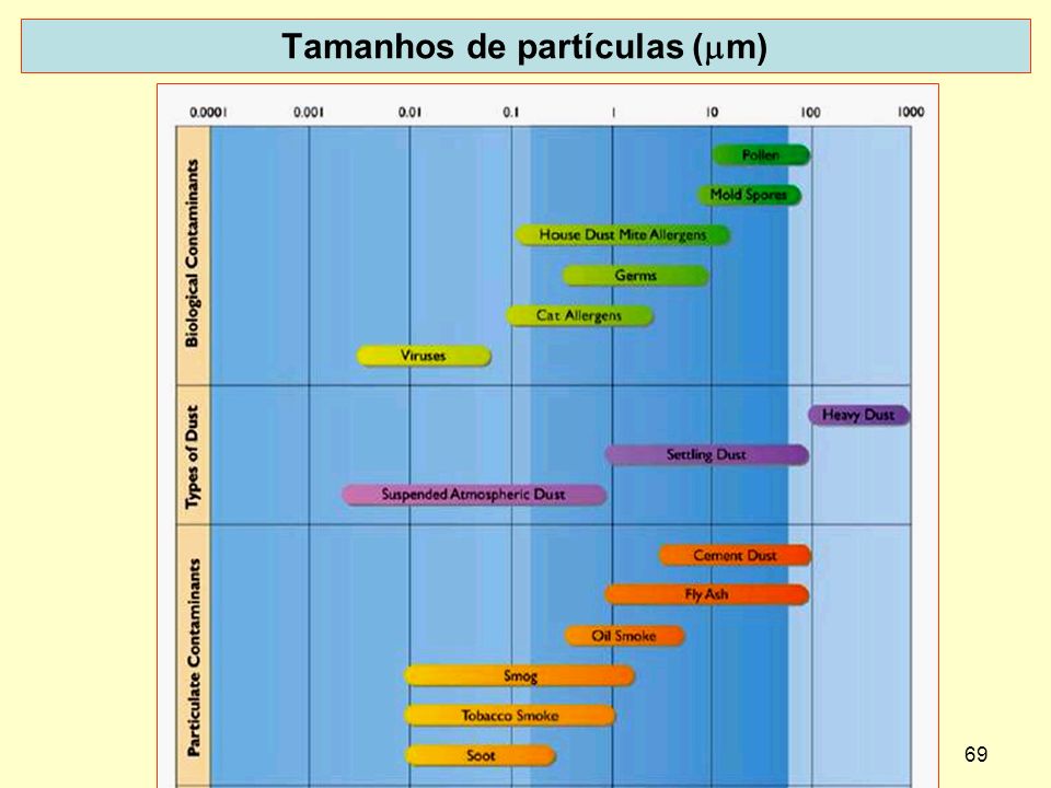
69
Tamanhos de partículas (mm)
70
Outra representação dos tamanhos
HEPA = high efficiency particulate air A high efficiency particulate air, or HEPA[1] (pronounced /ˈhɛpə/), filter is a type of high-efficiency air filter. What is HEPA Filtration? HEPA filtration was developed by the Atomic Energy Commission during World War II to remove radioactive particles from the air in manufacturing plants. Definition of HEPA Filter A HEPA filter must remove at least 99.97% of all airborne particles by particle count at a size of 0.3 microns which is one-300th the diameter of a human hair. It approaches total efficiency on all known organisms harmful to man. Common Uses for HEPA Filters In hospital operating rooms, burn centers, laboratories and manufacturers of critical products like computer chips, where particle and bacteria free air is mandatory, HEPA filtration systems are used to remove bacteria and other airborne contaminants. Filters are Maintenance Free HEPA filters require no cleaning or maintenance to maintain efficiency, and studies have proven that HEPA filters actually increase in efficiency with use over their 3 to 5 year life.
, filter is a type of high-efficiency air filter. What is HEPA Filtration HEPA filtration was developed by the Atomic Energy Commission during World War II to remove radioactive particles from the air in manufacturing plants. Definition of HEPA Filter. A HEPA filter must remove at least 99.97% of all airborne particles by particle count at a size of 0.3 microns which is one-300th the diameter of a human hair. It approaches total efficiency on all known organisms harmful to man. Common Uses for HEPA Filters. In hospital operating rooms, burn centers, laboratories and manufacturers of critical products like computer chips, where particle and bacteria free air is mandatory, HEPA filtration systems are used to remove bacteria and other airborne contaminants. Filters are Maintenance Free. HEPA filters require no cleaning or maintenance to maintain efficiency, and studies have proven that HEPA filters actually increase in efficiency with use over their 3 to 5 year life.")
71
Mais uma geral

72
Com que roupa vou?

80
MEMS = Micro Electro Mechanical System
Micro-Electro-Mechanical Systems (MEMS) is the integration of mechanical elements, sensors, actuators, and electronics on a common silicon substrate through microfabrication technology. While the electronics are fabricated using integrated circuit (IC) process sequences (e.g., CMOS, Bipolar, or BICMOS processes), the micromechanical components are fabricated using compatible "micromachining" processes that selectively etch away parts of the silicon wafer or add new structural layers to form the mechanical and electromechanical devices. MEMS promises to revolutionize nearly every product category by bringing together silicon-based microelectronics with micromachining technology, making possible the realization of complete systems-on-a-chip. MEMS is an enabling technology allowing the development of smart products, augmenting the computational ability of microelectronics with the perception and control capabilities of microsensors and microactuators and expanding the space of possible designs and applications. Microelectronic integrated circuits can be thought of as the "brains" of a system and MEMS augments this decision-making capability with "eyes" and "arms", to allow microsystems to sense and control the environment. Sensors gather information from the environment through measuring mechanical, thermal, biological, chemical, optical, and magnetic phenomena. The electronics then process the information derived from the sensors and through some decision making capability direct the actuators to respond by moving, positioning, regulating, pumping, and filtering, thereby controlling the environment for some desired outcome or purpose. Because MEMS devices are manufactured using batch fabrication techniques similar to those used for integrated circuits, unprecedented levels of functionality, reliability, and sophistication can be placed on a small silicon chip at a relatively low cost.
 is the integration of mechanical elements, sensors, actuators, and electronics on a common silicon substrate through microfabrication technology. While the electronics are fabricated using integrated circuit (IC) process sequences (e.g., CMOS, Bipolar, or BICMOS processes), the micromechanical components are fabricated using compatible micromachining processes that selectively etch away parts of the silicon wafer or add new structural layers to form the mechanical and electromechanical devices. MEMS promises to revolutionize nearly every product category by bringing together silicon-based microelectronics with micromachining technology, making possible the realization of complete systems-on-a-chip. MEMS is an enabling technology allowing the development of smart products, augmenting the computational ability of microelectronics with the perception and control capabilities of microsensors and microactuators and expanding the space of possible designs and applications. Microelectronic integrated circuits can be thought of as the brains of a system and MEMS augments this decision-making capability with eyes and arms , to allow microsystems to sense and control the environment. Sensors gather information from the environment through measuring mechanical, thermal, biological, chemical, optical, and magnetic phenomena. The electronics then process the information derived from the sensors and through some decision making capability direct the actuators to respond by moving, positioning, regulating, pumping, and filtering, thereby controlling the environment for some desired outcome or purpose. Because MEMS devices are manufactured using batch fabrication techniques similar to those used for integrated circuits, unprecedented levels of functionality, reliability, and sophistication can be placed on a small silicon chip at a relatively low cost.")
81
Engrenagens - acaro

82
Situação atual Design Fabricação Vendas de substratos Mascaras

83
NIST

84
Detecção de fluorescência

85
MEMS compatible micro-GRIN lenses for fiber to chip coupling of light
Michael Zickar, Wilfried Noell, Cornel Marxer, Nico de Rooij. Institute of Microtechnology (IMT), University of Neuchatel, Switzerland
, University of Neuchatel, Switzerland.")
86
Acoplamento lente grin –fibra óptica

87
Novos materiais óptica integrada
® material for the fabrication of integrated optical and opto-electronic devices. They exhibit low optical losses in the NIR range, especially at the most important wavelengths for optical communications (0.3 dB/cm at 1320 nm, 0.6 dB/cm at 1550 nm, without fluorination). The refractive index is easily and reproducibly tunable by mixing with an appropriate resin of different index. Moreover, process parameters have been optimized to achieve low cost packaging even in higher layer thicknesses (at present 100 mm within one step). In addition to a mechanistic study of the initial polycondensation reaction, examples for the applicability of the mentioned materials are given. Embedded channel waveguides have been produced as well as active devices like digital optical switches. ORMOCER®s in general are a class of hybrid inorganic/organic materials which amongst other utilizations prove highly valuable for application in packaging of integrated circuits. They show good optical and dielectric properties as well as good thermal stability (decomposition not below 270 °C). Furthermore, their chemical synthesis meets the requirements of microoptics and microelectronics industry since it enables highly reproducible low cost production of ORMOCER® micro structures. ORMOCER®s are manufactured in a two-step process, the first of which consists of the hydrolysis and polycondensation reaction of organically functionalized alkoxysilanes. The following reaction scheme (1) depicts the modified synthesis of the presented materials which focuses on alkoxylation. Diphenylsilanediol is reacted with 3-methacryloxypropyltrimethoxysilane under addition of a suitable condensation catalyst:
. The refractive index is easily and reproducibly tunable by mixing with an appropriate resin of different index. Moreover, process parameters have been optimized to achieve low cost packaging even in higher layer thicknesses (at present 100 mm within one step). In addition to a mechanistic study of the initial polycondensation reaction, examples for the applicability of the mentioned materials are given. Embedded channel waveguides have been produced as well as active devices like digital optical switches. ORMOCER®s in general are a class of hybrid inorganic/organic materials which amongst other utilizations prove highly valuable for application in packaging of integrated circuits. They show good optical and dielectric properties as well as good thermal stability (decomposition not below 270 °C). Furthermore, their chemical synthesis meets the requirements of microoptics and microelectronics industry since it enables highly reproducible low cost production of ORMOCER® micro structures. ORMOCER®s are manufactured in a two-step process, the first of which consists of the hydrolysis and polycondensation reaction of organically functionalized alkoxysilanes. The following reaction scheme (1) depicts the modified synthesis of the presented materials which focuses on alkoxylation. Diphenylsilanediol is reacted with 3-methacryloxypropyltrimethoxysilane under addition of a suitable condensation catalyst:")
88
Outro sistema Figure 6 (a) Manufacturing Optical Layers by Hot Embossing (Rib Cladding Process); (b) Manufacturing Optical Layers by Hot Embossing (Groove Filling Process) (Griese, 2002)
 Manufacturing Optical Layers by Hot Embossing (Rib Cladding Process); (b) Manufacturing Optical Layers by Hot Embossing (Groove Filling Process) (Griese, 2002)")
89
Microfone óptico Fig. 1: optical principle Fig. 2: basic build-up In the last years several transduction mechanisms for optical microphone technology have been developed. These are based on phase, polarisation and intensity modulation of light. The developed fiber optical microphone (FOM) is based on an intensity modulation and transduces airborne acoustic signals to light wave signals. This project was funded by “Micro System Technology (MST) Niedersachsen” in cooperation with “Sennheiser”, “Gesamtzentrum für Verkehr” (GZVB) and “Laser Laboratorium Göttingen” (LLG). Optical principle: The main principle of the optical microphone is to detect the vibration of a membrane using light. The emitted light from an LED is sent through an optical fiber onto the membrane which is furnished with a reflecting spot. The reflected light is coupled into the receiving fiber. When sound waves agitate the membrane it starts to vibrate, resulting in a toggling of the light spot on the receiving fiber. Consequentially a different intensity can be detected at the photo diode and is transformed into an electrical signal. Basic build-up: The design of the optical microphone basically consists of a mechanical part - housing, chip holder and buckling protection - and a functional part - membrane and positioning chip. The positioning chip serves as a micro-macro-interface for fiber optics and contains discrete or integrated optical components with high precision self-adjustment. Structuring the optical fibers to produce a prism by polishing the chip optical work bench with discrete optical components Integrated optics like lenses, prisms and waveguides
 is based on an intensity modulation and transduces airborne acoustic signals to light wave signals. This project was funded by Micro System Technology (MST) Niedersachsen in cooperation with Sennheiser , Gesamtzentrum für Verkehr (GZVB) and Laser Laboratorium Göttingen (LLG). Optical principle: The main principle of the optical microphone is to detect the vibration of a membrane using light. The emitted light from an LED is sent through an optical fiber onto the membrane which is furnished with a reflecting spot. The reflected light is coupled into the receiving fiber. When sound waves agitate the membrane it starts to vibrate, resulting in a toggling of the light spot on the receiving fiber. Consequentially a different intensity can be detected at the photo diode and is transformed into an electrical signal. Basic build-up: The design of the optical microphone basically consists of a mechanical part - housing, chip holder and buckling protection - and a functional part - membrane and positioning chip. The positioning chip serves as a micro-macro-interface for fiber optics and contains discrete or integrated optical components with high precision self-adjustment. Structuring the optical fibers to. produce a prism by polishing the chip. optical work bench with discrete. optical components. Integrated optics like lenses, prisms. and waveguides.")
90
Temos elétrons em sólidos e fótons em......materiais fotônicos
Cristais Fotônicos Elétrons de um lado e fótons do outro lado, junção de fóton + eletrônico Temos elétrons em sólidos e fótons em......materiais fotônicos

91
Cristais fotônicos Analogias Em Cristal Sólido Em Cristal Fotônico
Analogia entre cristal sólido e cristal fotônico. Analogias portadores estrutura bandas defeitos Em Cristal Sólido elétrons potencial periódico banda de energia defeitos: estados dentro da banda proibida Em Cristal Fotônico fótons modulação da constante dielétrica Banda de energia fotônica = photonic band gap (PBG) defeitos: estados dentro da banda com direcionalidade bem definida Escola André Svieca 2002? Cid Araujo Yablonovitch, PRL 58 (1987) 2059; John, PRL 58 (1987) 2486
 defeitos: estados dentro da banda com direcionalidade bem definida. Escola André Svieca 2002 Cid Araujo. Yablonovitch, PRL 58 (1987) 2059; John, PRL 58 (1987)")
92
Band Theory: “Bound” Electron Approach
For the total number N of atoms in a solid (1023 cm–3), N energy levels split apart within a width E. Leads to a band of energies for each initial atomic energy level (e.g. 1s energy band for 1s energy level). Two atoms Six atoms Solid of N atoms Electrons must occupy different energies due to Pauli Exclusion principle.
, N energy levels split apart within a width E. Leads to a band of energies for each initial atomic energy level (e.g. 1s energy band for 1s energy level). Two atoms. Six atoms. Solid of N atoms. Electrons must occupy different energies due to Pauli Exclusion principle.")
93
Filtro de Fabry-Perot C_MEMS
A C-MEMS Fabry-Perot filter consists of a micromachined silicon chip set comprising three or four individual chips. One chip has high-reflectivity and anti-reflective coatings on each side of its optically active area, which is surrounded by a large electrode. An elastomeric ring provides the filter's flexible element and provides a passive counterbalance to the electrostatic force. A second chip incorporates the drive electrodes, spaced several microns away from the movable mirror. Bonding the two pieces together with a reference mirror forms a basic mirror-driving unit with a reasonable voltage budget. An alternate configuration uses four chips to create two identical mirror-drive units. In either case, C-MEMS requires a low voltage budget to move the mirror along its normal optical axis and tune over the full range of channels in the C- or L-band at scan rates of at least 10 Hz. More important, it ensures a high degree of parallelism and a consistent filter shape with peak wavelength insertion losses under 2 dB. As a result of conditioning treatments, C-MEMS Fabry-Perot tunable filters have a simple calibration process. They only require a simple curve-fit method that yields accuracies of picometers. Such filters have demonstrated wavelength repeatability of 10 pm over the C-band tuning range. Like the optical networks they constitute, optical components confront diverse environmental conditions under which they must deliver consistent and predictable performance. The most common environmental factors are vibration and temperature change. Together, these factors present major design and packaging challenges for all devices placed in the optical path. Passive isolation-the common solution-proved insufficient to protect Fabry-Perot filters from residual environmental changes. A better approach is to configure filters with dual mirrors suspended in identical driving units. This enables common-mode cancellation principles to maintain zero relative differential movement for the mirror pairs-nulling environmental-vibration effects and yielding a stable filter peak position within several picometers when subjected to environmental vibration. This design has made C-MEMS tunable Fabry-Perot filters immune to the vibration encountered in normal operation. One effective design for C-MEMS Fabry-Perot filters maintains the core tunable filter chip set under a constant temperature condition. Heating the device to a higher temperature than the specified environmental extreme keeps the core filter chip set temperature stable. The supporting package temperature is still subject to environmental change and, if not properly isolated, mechanical thermal stress or stretch can impose wavelength drift. The solution: zero-stress or quasi-zero-stress attachment methods that minimize thermal stress spread into the optically active area. The approach enables reduction of peak wavelength temperature sensitivity to below 4 pm/ degrees C. If the device is configured to reoptimize every 30 minutes, it will lock the wavelength drift to less than plus/minus 30 pm under temperature-changing rates of 0.5 degrees C/minute. Performed more frequently, reoptimization can help reduce drift to less than 10 pm.

94
O seguinte é um seminário dado por Steven G
O seguinte é um seminário dado por Steven G. Johnson, MIT Applied Mathematics

95
From electrons to photons: Quantum-inspired modeling in nanophotonics
Steven G. Johnson, MIT Applied Mathematics

96
Nano-photonic media (l-scale)
strange waveguides & microcavities [B. Norris, UMN] [Assefa & Kolodziejski, MIT] 3d structures [Mangan, Corning] synthetic materials optical phenomena hollow-core fibers

97
can have a band gap: optical “insulators”
Photonic Crystals periodic electromagnetic media 1887 1987 can have a band gap: optical “insulators”

98
Electronic and Photonic Crystals
atoms in diamond structure dielectric spheres, diamond lattice wavevector photon frequency Periodic Medium Band Diagram Bloch waves: electron energy wavevector interacting: hard problem non-interacting: easy problem

99
Electronic & Photonic Modelling
• strongly interacting —tricky approximations • non-interacting (or weakly), —simple approximations (finite resolution) —any desired accuracy • lengthscale dependent (from Planck’s h) • scale-invariant —e.g. size 10 10 Option 1: Numerical “experiments” — discretize time & space … go Option 2: Map possible states & interactions using symmetries and conservation laws: band diagram
, —simple approximations. (finite resolution) —any desired accuracy. • lengthscale dependent. (from Planck’s h) • scale-invariant. —e.g. size 10 10. Option 1: Numerical experiments — discretize time & space … go. Option 2: Map possible states & interactions. using symmetries and conservation laws: band diagram.")
100
Fun with Math get rid of this mess First task:
dielectric function e(x) = n2(x) eigen-operator eigen-value eigen-state + constraint
 = n2(x) eigen-operator. eigen-value. eigen-state. + constraint.")
101
Electronic & Photonic Eigenproblems
nonlinear eigenproblem (V depends on e density ||2) simple linear eigenproblem (for linear materials) —many well-known computational techniques Hermitian = real E & w, … Periodicity = Bloch’s theorem…
 simple linear eigenproblem. (for linear materials) —many well-known. computational techniques. Hermitian = real E & w, … Periodicity = Bloch’s theorem…")
102
A 2d Model System dielectric “atom” square lattice, a a TM
e=12 (e.g. Si) square lattice, period a a a E TM H
 square lattice, period a. a. a. E. TM. H.")
103
Periodic Eigenproblems
if eigen-operator is periodic, then Bloch-Floquet theorem applies: can choose: planewave periodic “envelope” Corollary 1: k is conserved, i.e. no scattering of Bloch wave Corollary 2: given by finite unit cell, so w are discrete wn(k)
")
104
Solving the Maxwell Eigenproblem
Finite cell discrete eigenvalues wn Want to solve for wn(k), & plot vs. “all” k for “all” n, constraint: where: H(x,y) ei(kx – wt) 1 Limit range of k: irreducible Brillouin zone 2 Limit degrees of freedom: expand H in finite basis 3 Efficiently solve eigenproblem: iterative methods
, & plot vs. all k for all n, constraint: where: H(x,y) ei(kx – wt) 1. Limit range of k: irreducible Brillouin zone. 2. Limit degrees of freedom: expand H in finite basis. 3. Efficiently solve eigenproblem: iterative methods.")
105
Solving the Maxwell Eigenproblem: 1
Limit range of k: irreducible Brillouin zone 1 —Bloch’s theorem: solutions are periodic in k M kx ky first Brillouin zone = minimum |k| “primitive cell” X G irreducible Brillouin zone: reduced by symmetry 2 Limit degrees of freedom: expand H in finite basis 3 Efficiently solve eigenproblem: iterative methods

106
Solving the Maxwell Eigenproblem: 2a
Limit range of k: irreducible Brillouin zone 1 2 Limit degrees of freedom: expand H in finite basis (N) solve: finite matrix problem: 3 Efficiently solve eigenproblem: iterative methods
 solve: finite matrix problem: 3. Efficiently solve eigenproblem: iterative methods.")
107
Solving the Maxwell Eigenproblem: 2b
Limit range of k: irreducible Brillouin zone 1 2 Limit degrees of freedom: expand H in finite basis — must satisfy constraint: Planewave (FFT) basis Finite-element basis constraint, boundary conditions: Nédélec elements [ Nédélec, Numerische Math. 35, 315 (1980) ] constraint: nonuniform mesh, more arbitrary boundaries, complex code & mesh, O(N) uniform “grid,” periodic boundaries, simple code, O(N log N) [ figure: Peyrilloux et al., J. Lightwave Tech. 21, 536 (2003) ] 3 Efficiently solve eigenproblem: iterative methods
 basis. Finite-element basis. constraint, boundary conditions: Nédélec elements. [ Nédélec, Numerische Math. 35, 315 (1980) ] constraint: nonuniform mesh, more arbitrary boundaries, complex code & mesh, O(N) uniform grid, periodic boundaries, simple code, O(N log N) [ figure: Peyrilloux et al., J. Lightwave Tech. 21, 536 (2003) ] 3. Efficiently solve eigenproblem: iterative methods.")
108
Solving the Maxwell Eigenproblem: 3a
Limit range of k: irreducible Brillouin zone 1 2 Limit degrees of freedom: expand H in finite basis 3 Efficiently solve eigenproblem: iterative methods Slow way: compute A & B, ask LAPACK for eigenvalues — requires O(N2) storage, O(N3) time Faster way: — start with initial guess eigenvector h0 — iteratively improve — O(Np) storage, ~ O(Np2) time for p eigenvectors (p smallest eigenvalues)
 storage, O(N3) time. Faster way: — start with initial guess eigenvector h0. — iteratively improve. — O(Np) storage, ~ O(Np2) time for p eigenvectors. (p smallest eigenvalues)")
109
Solving the Maxwell Eigenproblem: 3b
Limit range of k: irreducible Brillouin zone 1 2 Limit degrees of freedom: expand H in finite basis 3 Efficiently solve eigenproblem: iterative methods Many iterative methods: — Arnoldi, Lanczos, Davidson, Jacobi-Davidson, …, Rayleigh-quotient minimization

110
Solving the Maxwell Eigenproblem: 3c
Limit range of k: irreducible Brillouin zone 1 2 Limit degrees of freedom: expand H in finite basis 3 Efficiently solve eigenproblem: iterative methods Many iterative methods: — Arnoldi, Lanczos, Davidson, Jacobi-Davidson, …, Rayleigh-quotient minimization for Hermitian matrices, smallest eigenvalue w0 minimizes: “variational theorem” minimize by preconditioned conjugate-gradient (or…)
")
111
Band Diagram of 2d Model System (radius 0.2a rods, e=12)
frequency w (2πc/a) = a / l irreducible Brillouin zone G X M G M E gap for n > ~1.75:1 TM X G H
 = a / l. irreducible Brillouin zone. G. X. M. G. M. E. gap for. n > ~1.75:1. TM. X. G. H.")
112
solutions are orthogonal and satisfy a variational theorem
Origin of the Band Gap Hermitian eigenproblems: solutions are orthogonal and satisfy a variational theorem Electronic Photonic field oscillations • minimize kinetic + potential energy (e.g. “bonding” state) • minimize: field in high e • higher bands orthogonal to lower — must oscillate (high kinetic) or be in low e (high potential) (e.g. “anti-bonding” state)
 • minimize: field in high e. • higher bands orthogonal to lower — must oscillate (high kinetic) or be in low e (high potential) (e.g. anti-bonding state)")
113
Origin of Gap in 2d Model System
orthogonal: node in high e Ez lives in high e G X M G Ez E gap for n > ~1.75:1 TM H – +

114
The Iteration Scheme is Important
(minimizing function of 104–108+ variables!) Steepest-descent: minimize (h + a f) over a … repeat Conjugate-gradient: minimize (h + a d) — d is f + (stuff): conjugate to previous search dirs Preconditioned steepest descent: minimize (h + a d) — d = (approximate A-1) f ~ Newton’s method Preconditioned conjugate-gradient: minimize (h + a d) — d is (approximate A-1) [f + (stuff)]
 Steepest-descent: minimize (h + a f) over a … repeat. Conjugate-gradient: minimize (h + a d) — d is f + (stuff): conjugate to previous search dirs. Preconditioned steepest descent: minimize (h + a d) — d = (approximate A-1) f ~ Newton’s method. Preconditioned conjugate-gradient: minimize (h + a d) — d is (approximate A-1) [f + (stuff)]")
115
The Iteration Scheme is Important
(minimizing function of ~40,000 variables) no preconditioning % error preconditioned conjugate-gradient no conjugate-gradient # iterations
 no preconditioning. % error. preconditioned. conjugate-gradient. no conjugate-gradient. # iterations.")
116
The Boundary Conditions are Tricky
E|| is continuous E is discontinuous (D = eE is continuous) Any single scalar e fails: (mean D) ≠ (any e) (mean E) Use a tensor e: E|| E e?
 Any single scalar e fails: (mean D) ≠ (any e) (mean E) Use a tensor e: E|| E e")
117
The e-averaging is Important
backwards averaging correct averaging changes order of convergence from ∆x to ∆x2 % error no averaging tensor averaging (similar effects in other E&M numerics & analyses) resolution (pixels/period)
 resolution (pixels/period)")
118
But, what can we do with the gap?
Gap, Schmap? a frequency w G X M G But, what can we do with the gap?

119
Intentional “defects” are good
microcavities waveguides (“wires”)
")
120
Intentional “defects” in 2d
(Same computation, with supercell = many primitive cells)
")
121
Microcavity Blues For cavities (point defects)
frequency-domain has its drawbacks: • Best methods compute lowest-w bands, but Nd supercells have Nd modes below the cavity mode — expensive • Best methods are for Hermitian operators, but losses requires non-Hermitian

122
Time-Domain Eigensolvers (finite-difference time-domain = FDTD)
Simulate Maxwell’s equations on a discrete grid, + absorbing boundaries (leakage loss) • Excite with broad-spectrum dipole ( ) source Dw signal processing Response is many sharp peaks, one peak per mode complex wn [ Mandelshtam, J. Chem. Phys. 107, 6756 (1997) ] decay rate in time gives loss
 • Excite with broad-spectrum dipole ( ) source. Dw. signal processing. Response is many. sharp peaks, one peak per mode. complex wn. [ Mandelshtam, J. Chem. Phys. 107, 6756 (1997) ] decay rate in time gives loss.")
123
Signal Processing is Tricky
complex wn ? a common approach: least-squares fit of spectrum fit to: FFT Decaying signal (t) Lorentzian peak (w)
 Lorentzian peak (w)")
124
problem: have to run long enough to completely decay
Fits and Uncertainty problem: have to run long enough to completely decay actual signal portion Portion of decaying signal (t) Unresolved Lorentzian peak (w) There is a better way, which gets complex w to > 10 digits
 Unresolved Lorentzian peak (w) There is a better way, which gets complex w to > 10 digits.")
125
Unreliability of Fitting Process
Resolving two overlapping peaks is near-impossible 6-parameter nonlinear fit (too many local minima to converge reliably) sum of two peaks There is a better way, which gets complex w for both peaks to > 10 digits w = i w = i Sum of two Lorentzian peaks (w)
 sum of two peaks. There is a better way, which gets. complex w. for both peaks. to > 10 digits. w = i. w = i. Sum of two Lorentzian peaks (w)")
126
Given time series yn, write:
Quantum-inspired signal processing (NMR spectroscopy): Filter-Diagonalization Method (FDM) [ Mandelshtam, J. Chem. Phys. 107, 6756 (1997) ] Given time series yn, write: …find complex amplitudes ak & frequencies wk by a simple linear-algebra problem! Idea: pretend y(t) is autocorrelation of a quantum system: say: time-∆t evolution-operator:
: Filter-Diagonalization Method (FDM) [ Mandelshtam, J. Chem. Phys. 107, 6756 (1997) ] Given time series yn, write: …find complex amplitudes ak & frequencies wk. by a simple linear-algebra problem! Idea: pretend y(t) is autocorrelation of a quantum system: say: time-∆t evolution-operator:")
127
Filter-Diagonalization Method (FDM)
[ Mandelshtam, J. Chem. Phys. 107, 6756 (1997) ] We want to diagonalize U: eigenvalues of U are eiw∆t …expand U in basis of |(n∆t)>: Umn given by yn’s — just diagonalize known matrix!
 ] We want to diagonalize U: eigenvalues of U are eiw∆t. …expand U in basis of |(n∆t)>: Umn given by yn’s — just diagonalize known matrix!")
128
Filter-Diagonalization Summary
[ Mandelshtam, J. Chem. Phys. 107, 6756 (1997) ] Umn given by yn’s — just diagonalize known matrix! A few omitted steps: —Generalized eigenvalue problem (basis not orthogonal) —Filter yn’s (Fourier transform): small bandwidth = smaller matrix (less singular) • resolves many peaks at once • # peaks not known a priori • resolve overlapping peaks • resolution >> Fourier uncertainty
 ] Umn given by yn’s — just diagonalize known matrix! A few omitted steps: —Generalized eigenvalue problem (basis not orthogonal) —Filter yn’s (Fourier transform): small bandwidth = smaller matrix (less singular) • resolves many peaks at once. • # peaks not known a priori. • resolve overlapping peaks. • resolution >> Fourier uncertainty.")
129
Do try this at home Bloch-mode eigensolver: Filter-diagonalization: Photonic-crystal tutorials (+ THIS TALK): /photons/tutorial/
: /photons/tutorial/")
130
Apresentação de temas

Apresentações semelhantes
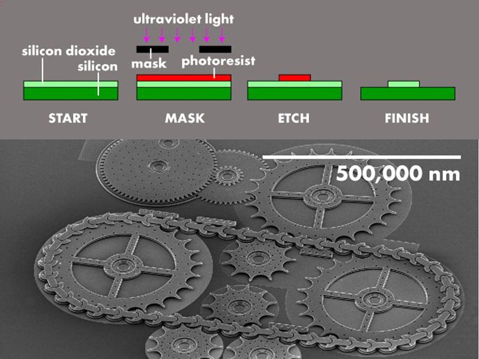
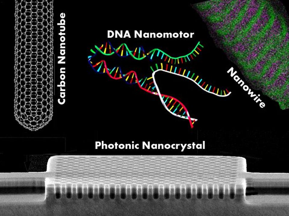
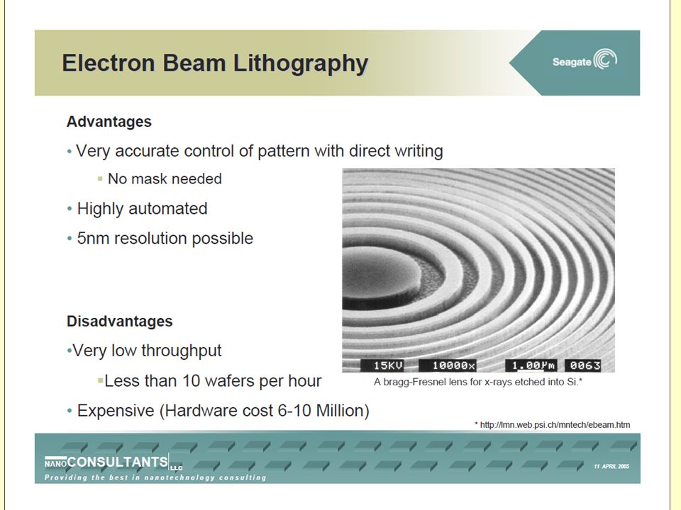
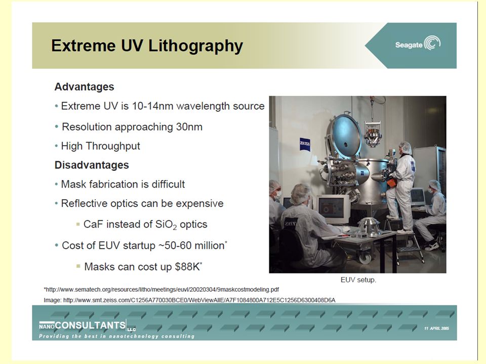
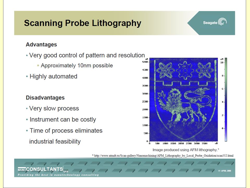
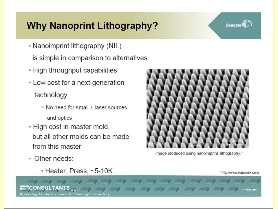
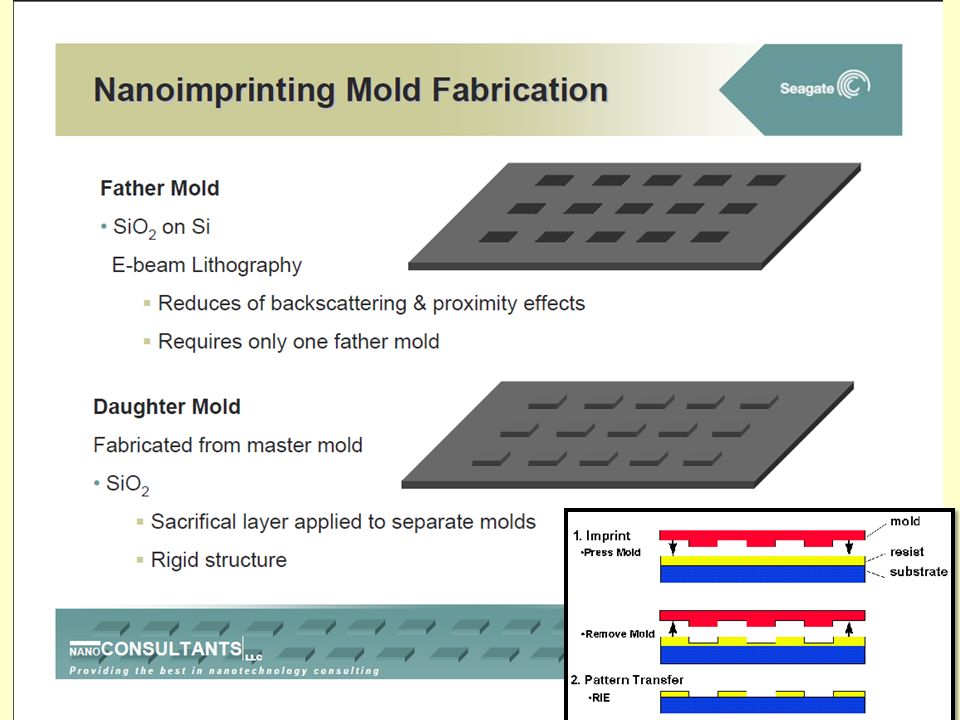
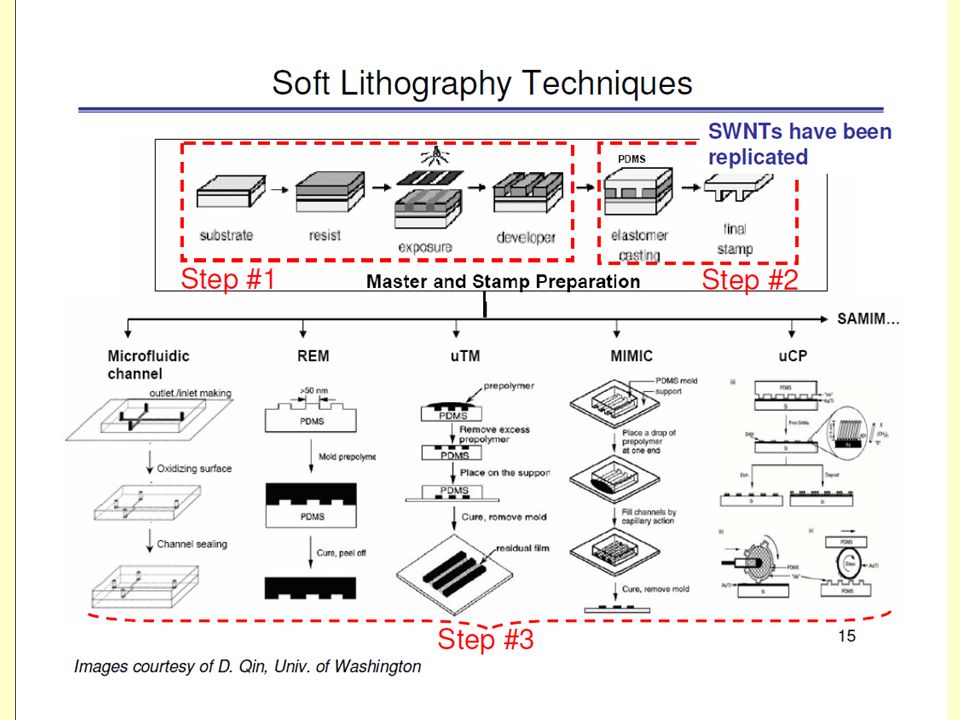

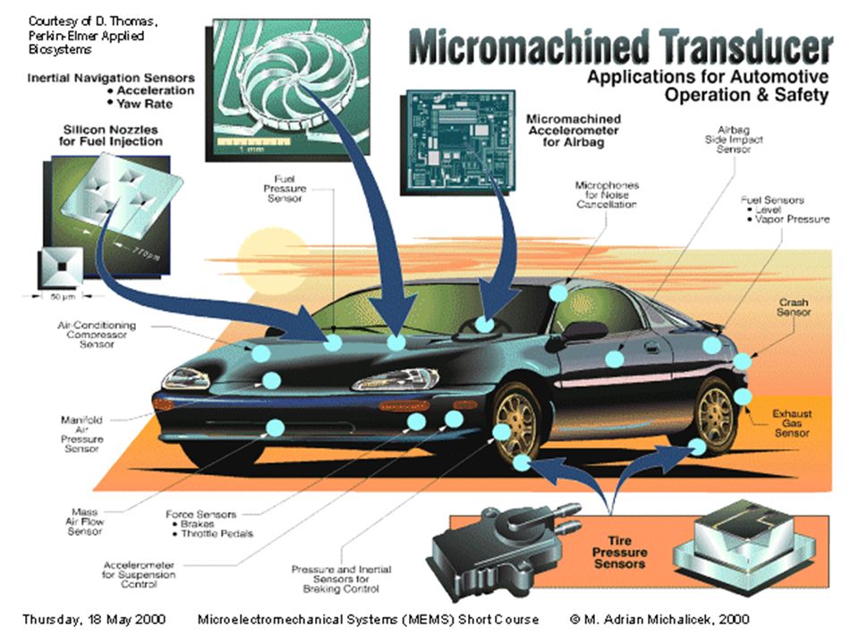


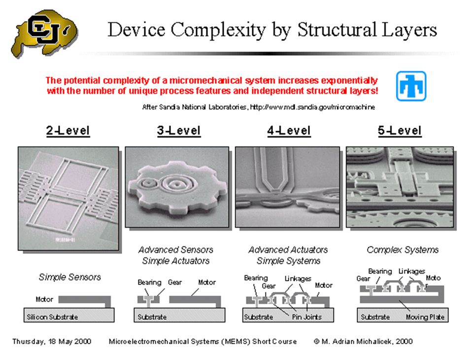
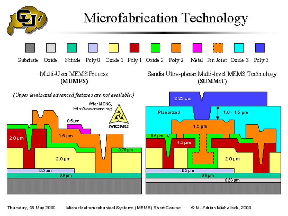
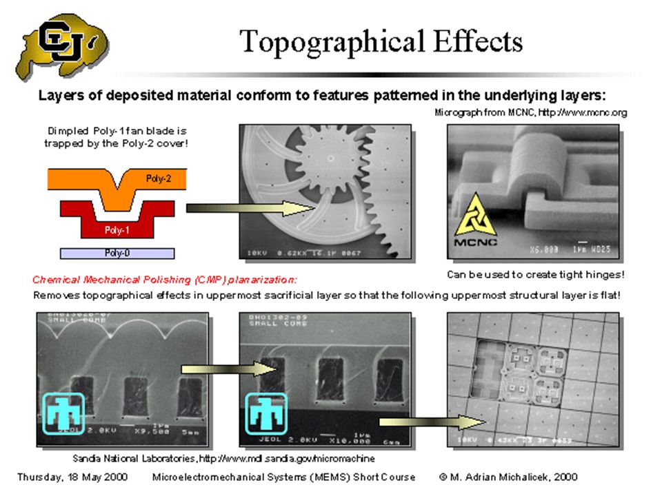
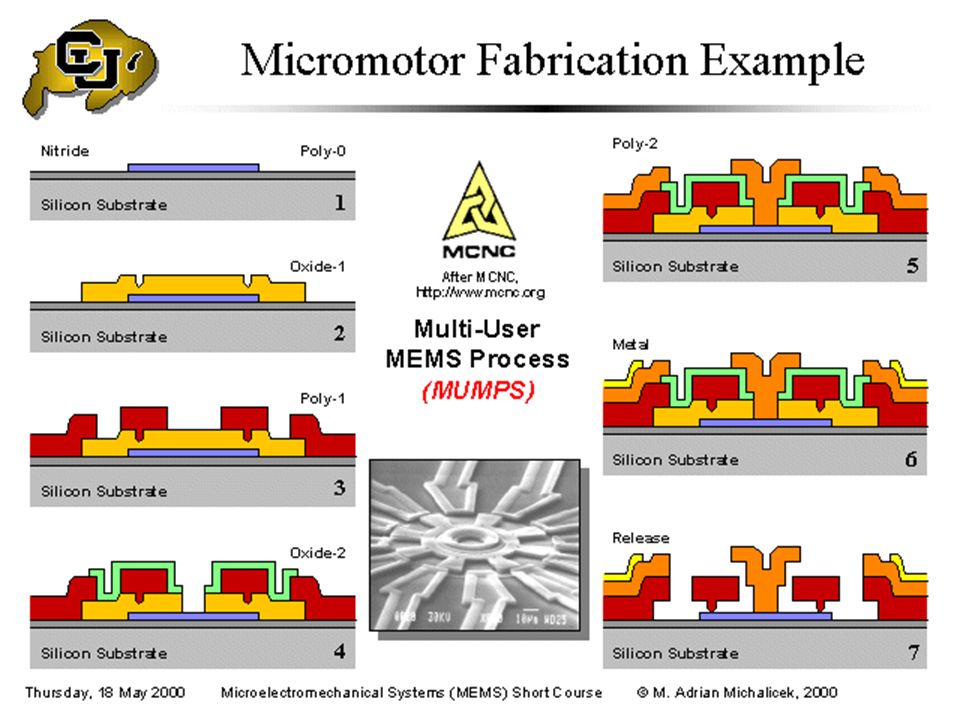

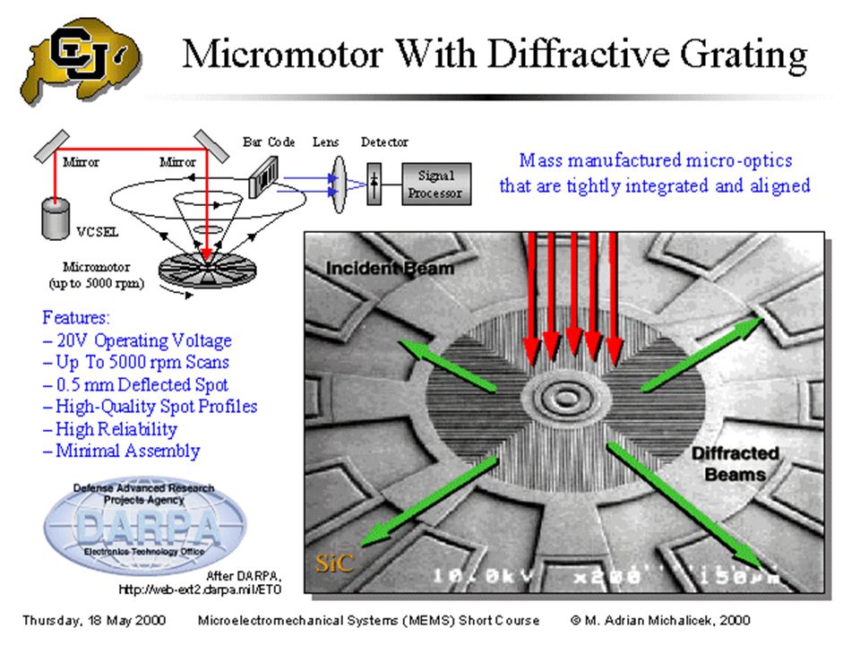
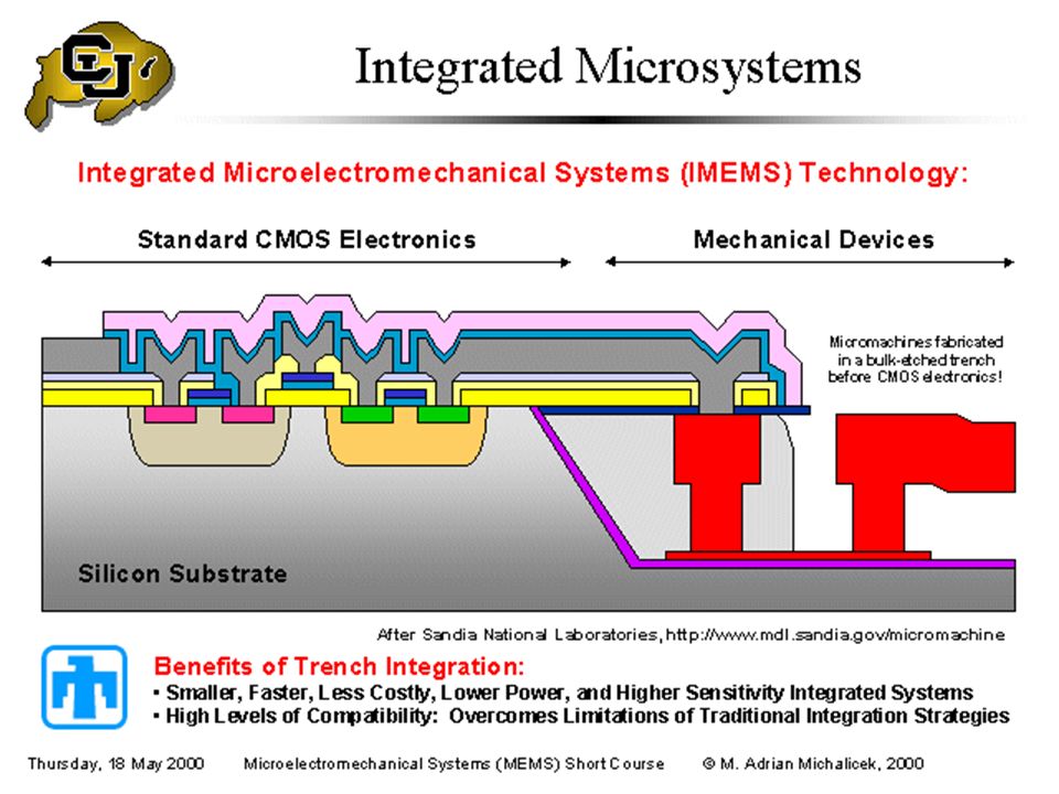

 – Lápides 1, 2, 3» «nomes gravados, 21 de Agosto de 2008» «Ultramar.TerraWeb»>")
![Z Y X [0 1 0] [1 0 1]. Z Y X [0 1 0] [1 0 1] a x y z b c For cubic: a = b = c = ao [001] [210] [100] [111] [120] 1½0 -2/311.](/1/46941/big_thumb.jpg "Z Y X [0 1 0] [1 0 1]. Z Y X [0 1 0] [1 0 1] a x y z b c For cubic: a = b = c = ao [001] [210] [100] [111] [120] 1½0 -2/311.>")


. Nenhuns direitos reservados, excepto para fins comerciais. Por favor, não coloque.>")
. Nenhuns direitos reservados, excepto para fins comerciais. Por favor, não coloque.>")


