Carregar apresentação
A apresentação está carregando. Por favor, espere

1
CURSO QF-435-SEGUNDO SEMENTRE 2008
AULA 3: NANOTUBOS DE CARBONO Prof. Dr. Nelson Durán IQ-UNICAMP CURSO QF-435-SEGUNDO SEMENTRE 2008 NANOMATERIAIS

2
MORFOLOGIA DOS SÓLIDOS
TAMANHO E MORFOLOGIA TAMANHO DOS SÓLIDOS O tamanho dos sólidos é importante quando tal parâmetro torna-se comparável a escala do fenômeno que está sendo observado - nanômetros Nanopartículas com tamanho e formas controladas têm sido sintetizadas Nano- tetraedro nanocubo nanocintas nanofitas Nano- bastões prismas nanofios nanotubos espirais Chem. Rev., 105 (4), 2005 MORFOLOGIA DOS SÓLIDOS Odair P. Ferreira Prof. Oswaldo L. Alves LQES – Laboratório de Química do Estado Sólido Instituto de Química - UNICAMP
, MORFOLOGIA DOS SÓLIDOS. Odair P. Ferreira. Prof. Oswaldo L. Alves. LQES – Laboratório de Química do. Estado Sólido Instituto de Química - UNICAMP.")
3
DIMENSIONALIDADE 3D 1D 0D 2D
Depende do tamanho relativo em diferentes direções espaciais; Silício Si/SiGe Carbono e Bi CdS Semicondutor bulk Quantum well/ sólidos lamelares Nanotubo e fio Quantum dots 3D 1D 0D 2D Odair P. Ferreira Prof. Oswaldo L. Alves LQES – Laboratório de Química do Estado Sólido Instituto de Química - UNICAMP

4
SISTEMAS UNIDIMENSIONAIS: NANOTUBOS E NANOBASTÕES
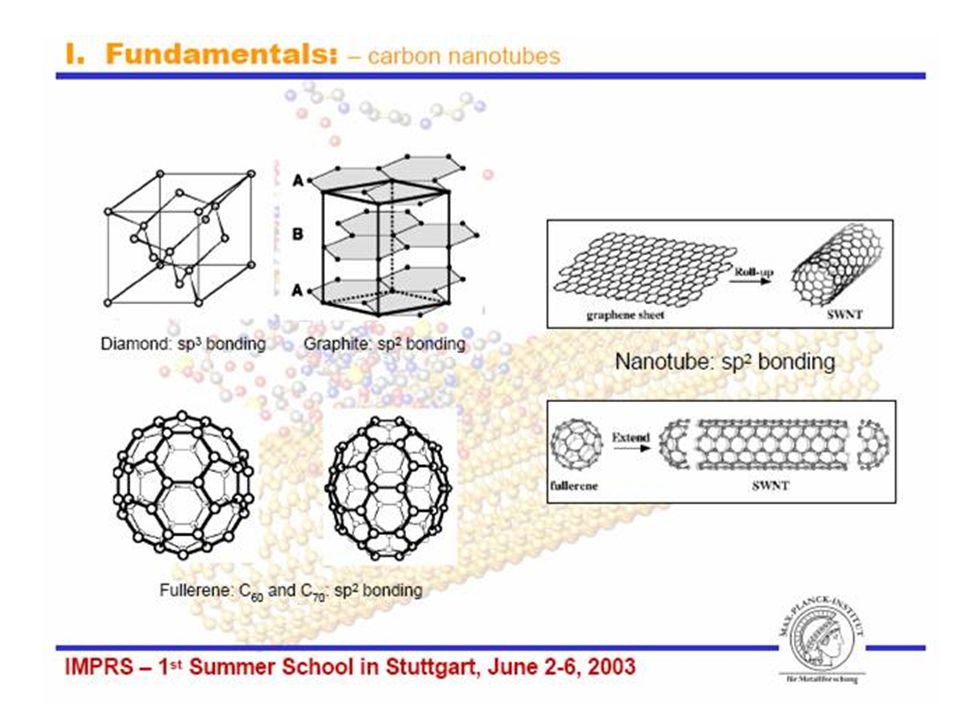
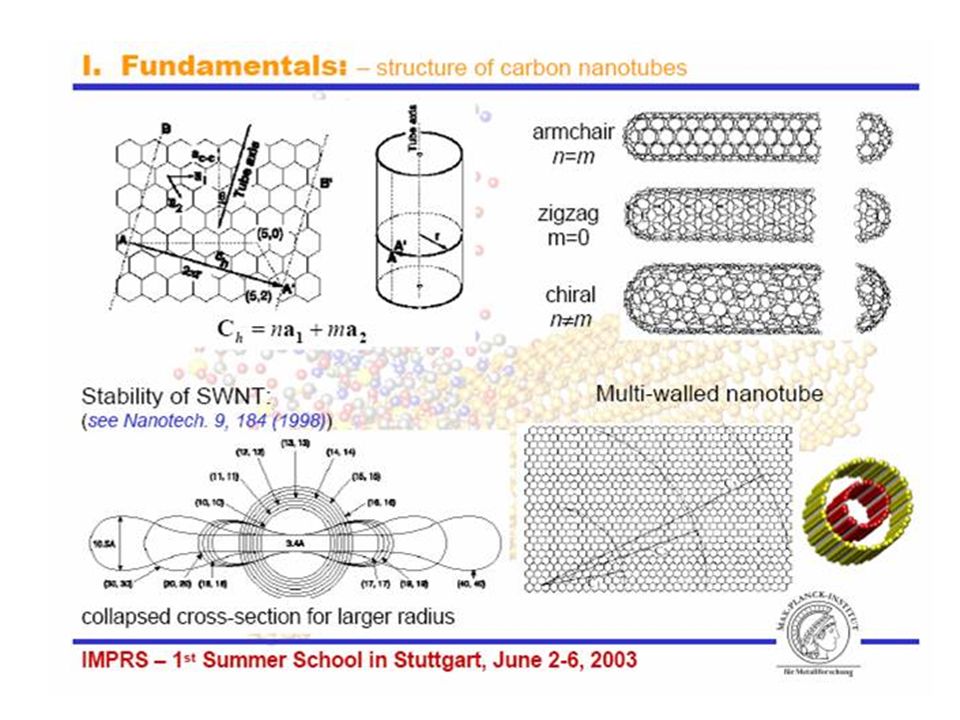
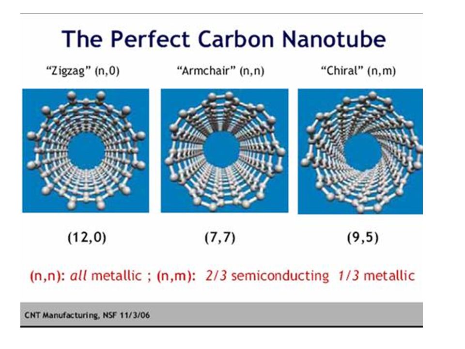
Nanotubos de Carbono Iijima, Nature, 359 (1991); Do ponto de vista estrutural Nanotubos seriam formados a partir de uma camada do grafite (sólido lamelar, 2D) que se fecha; (10,10) Força motriz ligações erráticas em átomos de carbono periféricos quando.
; Do ponto de vista estrutural Nanotubos seriam formados a partir de uma camada do grafite (sólido lamelar, 2D) que se fecha; (10,10) Força motriz ligações erráticas em átomos de carbono periféricos quando.")
5
NANOBASTÕES/NANOFIOS
Etapa chave para a obtenção de nanobastões controle da organização de átomos ou moléculas em uma direção preferencial; nanobastão/nanofio Diferentes maneiras para controlar a organização dos blocos construtores em nanobastões; 1 - Uso de templates; 2 - Nanotubo nanobastão ou nanobastões

7
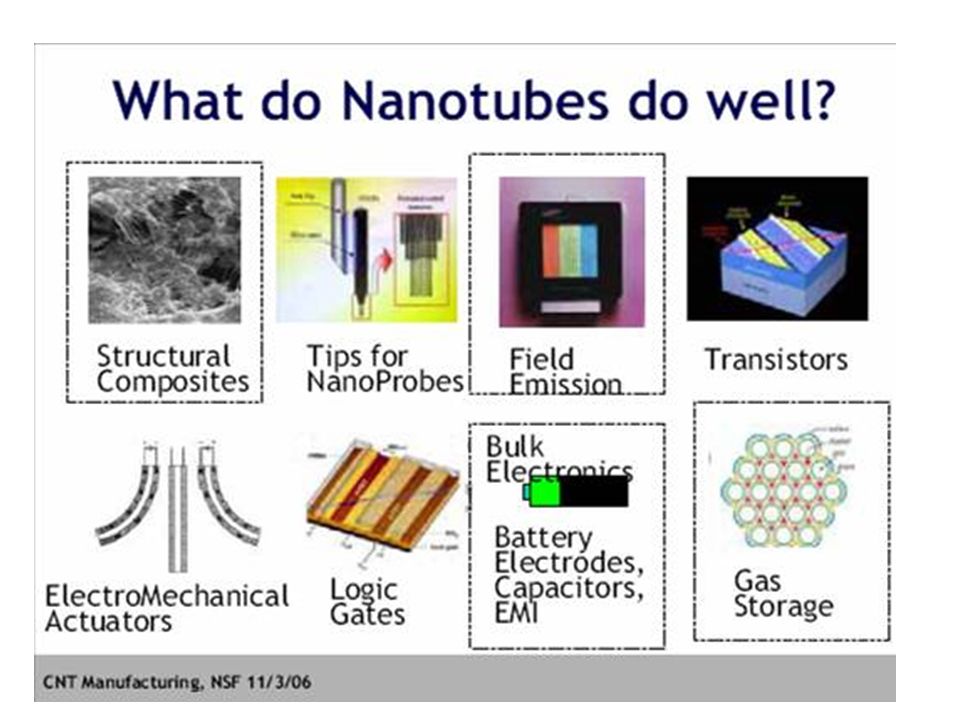
Ronaldo Marchese Congresso ABIQUIM Junho 2008

10
Anurak Vdomvech, Phys. Dep. Fac. Sci, Mahidol University, 2004

11
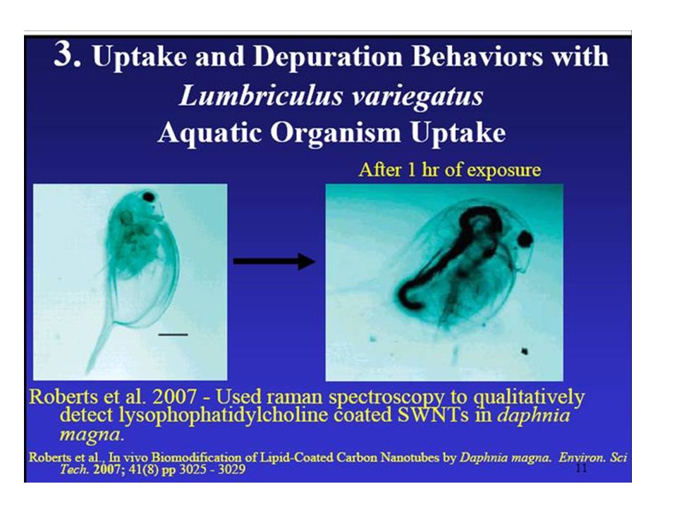
Bekyarova et al. J. Biomed. Nanotech. 1, 3-17 (2005)
")
12
Anurak Vdomvech, Phys. Dep. Fac. Sci, Mahidol University, 2004

13
Anurak Vdomvech, Phys. Dep. Fac. Sci, Mahidol University, 2004

14
Anurak Vdomvech, Phys. Dep. Fac. Sci, Mahidol University, 2004

15
Anurak Vdomvech, Phys. Dep. Fac. Sci, Mahidol University, 2004

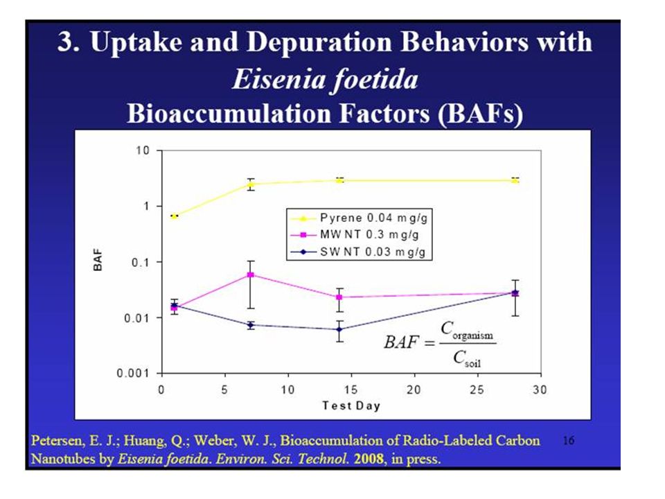
16
Ronaldo Marchese Congresso ABIQUIM
Junho 2008

20
Anurak Vdomvech, Phys. Dep. Fac. Sci, Mahidol University, 2004

21
Anurak Vdomvech, Phys. Dep. Fac. Sci, Mahidol University, 2004

22
Anurak Vdomvech, Phys. Dep. Fac. Sci, Mahidol University, 2004

23
Anurak Vdomvech, Phys. Dep. Fac. Sci, Mahidol University, 2004

24
Anurak Vdomvech, Phys. Dep. Fac. Sci, Mahidol University, 2004

25
Anurak Vdomvech, Phys. Dep. Fac. Sci, Mahidol University, 2004

26
Anurak Vdomvech, Phys. Dep. Fac. Sci, Mahidol University, 2004

27
Anurak Vdomvech, Phys. Dep. Fac. Sci, Mahidol University, 2004

28
Anurak Vdomvech, Phys. Dep. Fac. Sci, Mahidol University, 2004

29
Anurak Vdomvech, Phys. Dep. Fac. Sci, Mahidol University, 2004

30
Anurak Vdomvech, Phys. Dep. Fac. Sci, Mahidol University, 2004

31
J. Seetharamappa, S. Yellappa, and F. D’Souza
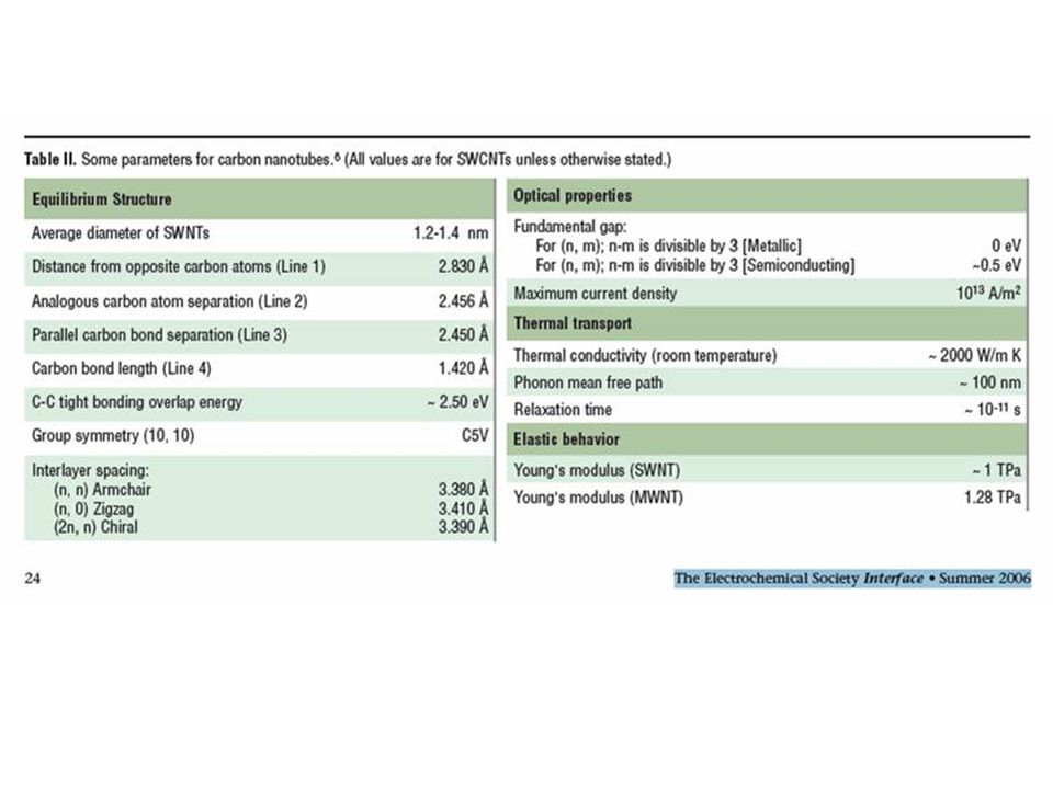
The Electrochemical Society Interface • Summer 2006

38
NANOECO-2008, Zwitzerland: www.empa/nanoECO

55
Surface characterization and functionalization of carbon nanofibers
A. Scanning probe microscopy SPM surveys small areas of surface with high lateral resolution, as opposed to techniques such as x-ray photoelectron spectroscopy XPS and infrared IR spectroscopy, which sample relatively large surface areas and yield mean values for surface properties. SPM techniques, including scanning tunneling microscopy STM and atomic force microscopy AFM, are capable of providing high surface sensitivity with atomic-level resolution; however, the yield of acceptable images is low and image interpretation can be difficult. When performing high-resolution scans, large numbers of images must be taken to ensure the data is representative. Klein et al. J. Appl. Phys. 103,

56
1. Scanning tunneling microscopy
STM can map the surfaces of electrically conductive materials with sub-Angstrom vertical resolution. 2. Atomic force microscopy The AFM has the inherent advantage in that it can generate high lateral resolution images with superb z-height discrimination from all types of surfaces—even those that are wet or insulating. Furthermore, the AFM exhibits sensitivity to chemical changes via molecular recognition and friction imaging, otherwise known as chemical force microscopy.

57
B. Infrared spectroscopy
IR spectroscopy, with the addition of the interferometer, is a robust and easy method for characterization of organic surfaces. Surface sensitive IR techniques can probe depths of a few centimeters to as shallow as 100 nm below the surface. Since CNFs are generally on the order of 20–200 nm in diameter, the spectra in this case convey “bulk” chemical information. However, this can be useful to distinguish which surface groups are present.

58
C. Electron spectroscopy
There are several ways of obtaining atomic composition and chemical bonding information from the surface. When x-rays of sufficient frequency energy interact with an atom, inner shell electrons in the atom are excited to outer, empty orbitals, or they may be ejected from the atom completely, so ionizing the atom. These electrons ejected by incident x-rays are called photoelectrons and can be detected by XPS. Likewise, an ultraviolet excitation source can also be used and the generated photoelectrons are measured by ultraviolet photoelectron spectroscopy UPS. Once a surface atom loses a photoelectron the atom desires to return to a relaxed state; thus the inner shell “hole” left by the photoelectron will then be filled by electrons from outer orbitals and their excess energy must be given off in the form of either x-ray fluorescence XRF or an ejected Auger electron. The ejected Auger electrons can be analyzed via Auger electron spectroscopy AES.

59
1. X-ray photoelectron spectroscopy
XPS is considered the “workhorse” of surface analysis because of its robustness and versatility. Using an x-ray source with energy in the keV range, the escape depth of core-level photoelectrons is only several atom layers deep with a lateral spatial resolution from 30 m to a few millimeters. The data produced permit the detection of all elements except hydrogen and helium with a sensitivity of better than 1 at. %. 2. Ultraviolet photoelectron spectroscopy UPS is similar to XPS but uses ultraviolet radiation 10–50 eV to excite valence-level photoelectrons of much lower kinetic energies. While the penetration depth and lateral spatial resolution are similar to XPS, the type of information obtained is quite different because UPS gives molecular orbital bonding and electronic structure information. 3. Auger electron spectroscopy As mentioned before, a fundamental advantage of AES is that the yield of Auger electrons is highest for the lighter elements such as C, Si, N, and O. In addition, the incident electron beam can be focused to a fine spot giving excellent lateral spatial resolution on the order of a few tens of nanometers.

60
D. Electron microscopy Secondary electron microscopy SEM is perhaps the most frequently used method of characterizing the morphological structure and topography of a sample. TEM and scanning transmission electron microscopy STEM convey information about the nanostructure as a whole, but can also show the presence of surface layers and reveal the atomic structure of the surface interface by high-resolution TEM HRTEM. A common companion tool to both the SEM and the TEM is an energy dispersive x-ray EDX spectrometer, which readily gives the elemental composition of the sample and can also be useful in generating elemental maps. Electron energy loss spectroscopy EELS is a valuable analytical tool both for determining the composition of TEM specimens and for providing information about the valence state and electronic structure of the material under examination.

61
1. Scanning electron microscopy
Although scanning electron microscopy is the most widely used surface imaging technique, the depth from which the relevant secondary electrons typically escape usually ranging from 5 to 50 nm deep depending on the material results in the image containing both surface and bulk information. Image contrast and brightness can also be ambiguous and not quantitatively topographical; edges are often highlighted and surface charging can result in large fluctuations in signal level as well as in distortions of the scan raster. 2. Energy dispersive x-ray microanalysis EDX measures the energies of the characteristic x-rays generated from ionizations induced within the specimen in an electron microscope. Each element emits a unique fingerprint of x-ray energies related to the difference in binding energies of the electron shells involved in the relaxation process. Therefore, EDX is a tool often used along with electron microscopy imaging to give complementary chemical information.

62
3. Transmission electron microscopy
The surface as well as internal structure of CNFs can be analyzed using STEM or TEM. Both real space “image” and reciprocal space “diffraction” data, together with chemical and electronic analytical information derived from EDX or EELS, can be obtained from the same nanoscale area. The TEM and STEM therefore provide a wide and deep range of data about the specimen of interest. 4. Electron energy loss spectroscopy EELS measures the energy spectrum of the electron beam transmitted through the sample in the TEM or STEM. The spectrum contains chemical data, which are complementary to those derived from EDX, but with much higher sensitivity for the lower atomic number elements Z20. In addition, other phenomena such as plasmon excitations, ionization edge fine structure, and extended fine structure effects provide a detailed look at valence, bond structures, radial distribution functions, and other descriptors of microstructure on the atomic scale

63
E. Secondary ion mass spectrometry
Secondary ion mass spectrometry SIMS is a powerful characterization tool with outstanding surface sensitivity on the scale of a few atomic layers. SIMS also provides detection limits surpassing those attainable with XPS. The drawbacks of SIMS include sample charging and the complexity of the instrumentation and data analysis.

64
1. Dynamic SIMS In dynamic SIMS, a continuous, high-flux stream of primary ions having an energy of 1–20 keV bombards the surface and fragments it as much as possible to maximize the generation of charged atomic species. 2. Static SIMS In contrast to dynamic SIMS, the goal in static SIMS is to maintain the molecular integrity of the surface fragments as much as possible. Therefore, a pulsed source is often used, the primary beam flux is reduced, and the beam is rastered to generate larger charged sample fragments. Because many of the detected species are not distinctly identifiable, S-SIMS is only qualitative.

65
F. Temperature-programed desorption
Temperature-programed desorption TPD, also called thermal desorption spectroscopy TDS, is a method of characterizing adsorbed surface species by heating the sample while under vacuum and simultaneously detecting the residual gas by means of a mass spectrometer. As the temperature rises, certain absorbed species will have enough energy to escape or desorb from the surface and will be detected as a rise in pressure for a particular mass component.

66
G. Atom probe The atom probe is an instrument that combines both a probe-aperture field ion microscope with atomically high resolution and a mass spectrometer with single particle sensitivity . Over the years, the atom probe has evolved to include the unique capability of atomic layer-by-layer depth profiling using time-of-flight mass analysis. The scanning atom probe SAP works by field evaporating surface atoms from the sample for mass analysis; thus for field enhancement purposes, protruding, high aspect ratio structures are ideal.

Apresentações semelhantes


. Metallic bonding is essentially covalent bonding with delocalized electrons.>")
 SEGUNDO NOVOS ESTRATOS VITÓRIA, ES – OUTUBRO 2008 Kenneth Camargo – IMS/UERJ Cláudia Medina – IESC/UFRJ.>")


