Carregar apresentação
A apresentação está carregando. Por favor, espere

1
Resumo aula anterior + apresentações
Apresntação por parte dos alunos: NEP, D* (Gustavo) Responsividade (sensitividade) (Tarcísio) CIE (Gabriel) Figuras de mérito dos detectores: NEP, R, tc, D Dois tipos de detectores: Fotônicos Térmicos Detectores fotônicos: Fotoemissivos: tubos a vácuo, efeito fotoelétrico, channeltron, PMT
 Responsividade (sensitividade) (Tarcísio) CIE (Gabriel) Figuras de mérito dos detectores: NEP, R, tc, D. Dois tipos de detectores: Fotônicos. Térmicos. Detectores fotônicos: Fotoemissivos: tubos a vácuo, efeito fotoelétrico, channeltron, PMT.")
2
Nosso último assunto foi sobre fotodiodo de silício e channeltron

3
Fotodiodo de silício

4
Detectores fotovoltaicos

5
Resposta espectral de D* de detectores fotovoltaicos

6
O mesmo principio é usado na obtenção de células solares

7
A = encapsulamento que sela a célula do ambiente externo, pode ser vidro ou plástico B = grade de contato, bom material condutor, que pode servir como coletor de elétrons C = Camada Anti-Refletora, com índice de refração e espessura apropriados, guia a luz para dentro da célula, evitando que a luz incidente seja refletida para fora da célula D = silício tipo -n (e.g. P ou As como impurezas) E = silício tipo -p (e.g. B) F = contato metálico recobrindo toda a base da célula HOW SOLAR CELLS WORK - SOLAR CELL OVERVIEW SOLAR CELLS, How They Work The solar cell offers a limitless and environmentally friendly source of electricity. The solar cell, is able to create electricity directly from photons. A photon can be thought of as a packet of light and the amount of energy in a photon is proportional to the wavelength of light. A. Encapsulate - The encapsulate, made of glass or other clear material such clear plastic, seals the cell from the external environment. B. Contact Grid- The contact grid is made of a good conductor, such as a metal, and it serves as a collector of electrons. C. The Antireflective Coating (AR Coating)- Through a combination of a favorable refractive index, and thickness, this layer serves to guide light into the solar cell. Without this layer, much of the light would simply bounce off the surface. D. N-Type Silicon - N-type silicon is created by doping (contaminating) the Si with compounds that contain one more valence electrons* than Si does, such as with either Phosphorus or Arsenic. Since only four electrons are required to bond with the four adjacent silicon atoms, the fifth valence electron is available for conduction. E. P-Type Silicon- P-type silicon is created by doping with compounds containing one less valence electrons* than Si does, such as with Boron. When silicon (four valence electrons) is doped with atoms that have one less valence electrons (three valence electrons), only three electrons are available for bonding with four adjacent silicon atoms, therefore an incomplete bond (hole) exists which can attract an electron from a nearby atom. Filling one hole creates another hole in a different Si atom. This movement of holes is available for conduction. F. Back Contact - The back contact, made out of a metal, covers the entire back surface of the solar cell and acts as a conductor. *[ A valence electron is an electron found in the outermost electron shell. An element containing more valence electrons will try to donate valence electrons to an element containing fewer valence electrons.] * A photon's path through the solar cell. After a photon makes its way through the encapsulate it encounters the antireflective layer. The antireflective layer channels the photon into the lower layers of the solar cell. Click on the following link if you would like to learn about SPECMAT's novel room temperature wet chemical growth antireflective layer (RTWCG - AR). Once the photon passes the antireflective layer, it will either hit the silicon surface of the solar cell or the contact grid metallization. The metallization, being opaque, lowers the number of photons reaching the Si surface. The contact grid must be large enough to collect electrons yet cover as little of the solar cell's surface, allowing more photons to penetrate. A Photon causes the Photoelectric Effect*. The photon's energy transfers to the valence electron of an atom in the n-type Si layer. That energy allows the valence electron to escape its orbit leaving behind a hole. In the n-type silicon layer, the free electrons are called majority carriers whereas the holes are called minority carriers. As the term "carrier" implies, both are able to move throughout the silicon layer of the solar cell, and so are said to be mobile. Inversely, in the p-type silicon layer, electrons are termed minority carriers and holes are termed majority carriers, and of course are also mobile. *[ The photoelectric effect is simply defined as an experimentally measurable effect where a metal emits electrons when hit by photons..] * The p-n junction. The region in the solar cell where the n-type and p-type Si layers meet is called the p-n junction. As you may have already guessed, the p-type silicon layer contains more positive charges, called holes, and the n-type silicon layer contains more negative charges, or electrons. When p-type and n-type materials are placed in contact with each other, current will flow readily in one direction (forward biased) but not in the other (reverse biased). An interesting interaction occurs at the p-n junction of a darkened solar cell. Extra valence electrons in the n-type layer move into the p-type layer filling the holes in the p-type layer forming what is called a depletion zone. The depletion zone does not contain any mobile positive or negative charges. Moreover, this zone keeps other charges from the p and n-type layers from moving across it. So, to recap, a region depleted of carriers is left around the junction, and a small electrical imbalance exists inside the solar cell. This electrical imbalance amounts to about 0.6 to 0.7 volts. So due to the p-n junction, a built in electric field is always present across the solar cell. P = V × I When photons hit the solar cell, freed electrons (-) attempt to unite with holes on the p-type layer. The p-n junction, a one-way road, only allows the electrons to move in one direction. If we provide an external conductive path, electrons will flow through this path to their original (p-type) side to unite with holes. The electron flow provides the current ( I ), and the cell's electric field causes a voltage ( V ). With both current and voltage, we have power ( P ), which is just the product of the two. Therefore, when an external load (such as an electric bulb) is connected between the front and back contacts, electricity flows in the cell, working for us along the way.
 E = silício tipo -p (e.g. B) F = contato metálico recobrindo toda a base da célula. HOW SOLAR CELLS WORK - SOLAR CELL OVERVIEW. SOLAR CELLS, How They Work. The solar cell offers a limitless and environmentally friendly source of electricity. The solar cell, is able to create electricity directly from photons. A photon can be thought of as a packet of light and the amount of energy in a photon is proportional to the wavelength of light. A. Encapsulate - The encapsulate, made of glass or other clear material such clear plastic, seals the cell from the external environment. B. Contact Grid- The contact grid is made of a good conductor, such as a metal, and it serves as a collector of electrons. C. The Antireflective Coating (AR Coating)- Through a combination of a favorable refractive index, and thickness, this layer serves to guide light into the solar cell. Without this layer, much of the light would simply bounce off the surface. D. N-Type Silicon - N-type silicon is created by doping (contaminating) the Si with compounds that contain one more valence electrons* than Si does, such as with either Phosphorus or Arsenic. Since only four electrons are required to bond with the four adjacent silicon atoms, the fifth valence electron is available for conduction. E. P-Type Silicon- P-type silicon is created by doping with compounds containing one less valence electrons* than Si does, such as with Boron. When silicon (four valence electrons) is doped with atoms that have one less valence electrons (three valence electrons), only three electrons are available for bonding with four adjacent silicon atoms, therefore an incomplete bond (hole) exists which can attract an electron from a nearby atom. Filling one hole creates another hole in a different Si atom. This movement of holes is available for conduction. F. Back Contact - The back contact, made out of a metal, covers the entire back surface of the solar cell and acts as a conductor. *[ A valence electron is an electron found in the outermost electron shell. An element containing more valence electrons will try to donate valence electrons to an element containing fewer valence electrons.] * A photon s path through the solar cell. After a photon makes its way through the encapsulate it encounters the antireflective layer. The antireflective layer channels the photon into the lower layers of the solar cell. Click on the following link if you would like to learn about SPECMAT s novel room temperature wet chemical growth antireflective layer (RTWCG - AR). Once the photon passes the antireflective layer, it will either hit the silicon surface of the solar cell or the contact grid metallization. The metallization, being opaque, lowers the number of photons reaching the Si surface. The contact grid must be large enough to collect electrons yet cover as little of the solar cell s surface, allowing more photons to penetrate. A Photon causes the Photoelectric Effect*. The photon s energy transfers to the valence electron of an atom in the n-type Si layer. That energy allows the valence electron to escape its orbit leaving behind a hole. In the n-type silicon layer, the free electrons are called majority carriers whereas the holes are called minority carriers. As the term carrier implies, both are able to move throughout the silicon layer of the solar cell, and so are said to be mobile. Inversely, in the p-type silicon layer, electrons are termed minority carriers and holes are termed majority carriers, and of course are also mobile. *[ The photoelectric effect is simply defined as an experimentally measurable effect where a metal emits electrons when hit by photons..] * The p-n junction. The region in the solar cell where the n-type and p-type Si layers meet is called the p-n junction. As you may have already guessed, the p-type silicon layer contains more positive charges, called holes, and the n-type silicon layer contains more negative charges, or electrons. When p-type and n-type materials are placed in contact with each other, current will flow readily in one direction (forward biased) but not in the other (reverse biased). An interesting interaction occurs at the p-n junction of a darkened solar cell. Extra valence electrons in the n-type layer move into the p-type layer filling the holes in the p-type layer forming what is called a depletion zone. The depletion zone does not contain any mobile positive or negative charges. Moreover, this zone keeps other charges from the p and n-type layers from moving across it. So, to recap, a region depleted of carriers is left around the junction, and a small electrical imbalance exists inside the solar cell. This electrical imbalance amounts to about 0.6 to 0.7 volts. So due to the p-n junction, a built in electric field is always present across the solar cell. P = V × I. When photons hit the solar cell, freed electrons (-) attempt to unite with holes on the p-type layer. The p-n junction, a one-way road, only allows the electrons to move in one direction. If we provide an external conductive path, electrons will flow through this path to their original (p-type) side to unite with holes. The electron flow provides the current ( I ), and the cell s electric field causes a voltage ( V ). With both current and voltage, we have power ( P ), which is just the product of the two. Therefore, when an external load (such as an electric bulb) is connected between the front and back contacts, electricity flows in the cell, working for us along the way.")
8
Numa maneira ilustrativa
HOW SOLAR CELLS WORK - SOLAR CELL OVERVIEW SOLAR CELLS, How They Work The solar cell offers a limitless and environmentally friendly source of electricity. The solar cell, is able to create electricity directly from photons. A photon can be thought of as a packet of light and the amount of energy in a photon is proportional to the wavelength of light. A. Encapsulate - The encapsulate, made of glass or other clear material such clear plastic, seals the cell from the external environment. B. Contact Grid- The contact grid is made of a good conductor, such as a metal, and it serves as a collector of electrons. C. The Antireflective Coating (AR Coating)- Through a combination of a favorable refractive index, and thickness, this layer serves to guide light into the solar cell. Without this layer, much of the light would simply bounce off the surface. D. N-Type Silicon - N-type silicon is created by doping (contaminating) the Si with compounds that contain one more valence electrons* than Si does, such as with either Phosphorus or Arsenic. Since only four electrons are required to bond with the four adjacent silicon atoms, the fifth valence electron is available for conduction. E. P-Type Silicon- P-type silicon is created by doping with compounds containing one less valence electrons* than Si does, such as with Boron. When silicon (four valence electrons) is doped with atoms that have one less valence electrons (three valence electrons), only three electrons are available for bonding with four adjacent silicon atoms, therefore an incomplete bond (hole) exists which can attract an electron from a nearby atom. Filling one hole creates another hole in a different Si atom. This movement of holes is available for conduction. F. Back Contact - The back contact, made out of a metal, covers the entire back surface of the solar cell and acts as a conductor. *[ A valence electron is an electron found in the outermost electron shell. An element containing more valence electrons will try to donate valence electrons to an element containing fewer valence electrons.] * A photon's path through the solar cell. After a photon makes its way through the encapsulate it encounters the antireflective layer. The antireflective layer channels the photon into the lower layers of the solar cell. Click on the following link if you would like to learn about SPECMAT's novel room temperature wet chemical growth antireflective layer (RTWCG - AR). Once the photon passes the antireflective layer, it will either hit the silicon surface of the solar cell or the contact grid metallization. The metallization, being opaque, lowers the number of photons reaching the Si surface. The contact grid must be large enough to collect electrons yet cover as little of the solar cell's surface, allowing more photons to penetrate. A Photon causes the Photoelectric Effect*. The photon's energy transfers to the valence electron of an atom in the n-type Si layer. That energy allows the valence electron to escape its orbit leaving behind a hole. In the n-type silicon layer, the free electrons are called majority carriers whereas the holes are called minority carriers. As the term "carrier" implies, both are able to move throughout the silicon layer of the solar cell, and so are said to be mobile. Inversely, in the p-type silicon layer, electrons are termed minority carriers and holes are termed majority carriers, and of course are also mobile. *[ The photoelectric effect is simply defined as an experimentally measurable effect where a metal emits electrons when hit by photons..] * The p-n junction. The region in the solar cell where the n-type and p-type Si layers meet is called the p-n junction. As you may have already guessed, the p-type silicon layer contains more positive charges, called holes, and the n-type silicon layer contains more negative charges, or electrons. When p-type and n-type materials are placed in contact with each other, current will flow readily in one direction (forward biased) but not in the other (reverse biased). An interesting interaction occurs at the p-n junction of a darkened solar cell. Extra valence electrons in the n-type layer move into the p-type layer filling the holes in the p-type layer forming what is called a depletion zone. The depletion zone does not contain any mobile positive or negative charges. Moreover, this zone keeps other charges from the p and n-type layers from moving across it. So, to recap, a region depleted of carriers is left around the junction, and a small electrical imbalance exists inside the solar cell. This electrical imbalance amounts to about 0.6 to 0.7 volts. So due to the p-n junction, a built in electric field is always present across the solar cell. P = V × I When photons hit the solar cell, freed electrons (-) attempt to unite with holes on the p-type layer. The p-n junction, a one-way road, only allows the electrons to move in one direction. If we provide an external conductive path, electrons will flow through this path to their original (p-type) side to unite with holes. The electron flow provides the current ( I ), and the cell's electric field causes a voltage ( V ). With both current and voltage, we have power ( P ), which is just the product of the two. Therefore, when an external load (such as an electric bulb) is connected between the front and back contacts, electricity flows in the cell, working for us along the way.
- Through a combination of a favorable refractive index, and thickness, this layer serves to guide light into the solar cell. Without this layer, much of the light would simply bounce off the surface. D. N-Type Silicon - N-type silicon is created by doping (contaminating) the Si with compounds that contain one more valence electrons* than Si does, such as with either Phosphorus or Arsenic. Since only four electrons are required to bond with the four adjacent silicon atoms, the fifth valence electron is available for conduction. E. P-Type Silicon- P-type silicon is created by doping with compounds containing one less valence electrons* than Si does, such as with Boron. When silicon (four valence electrons) is doped with atoms that have one less valence electrons (three valence electrons), only three electrons are available for bonding with four adjacent silicon atoms, therefore an incomplete bond (hole) exists which can attract an electron from a nearby atom. Filling one hole creates another hole in a different Si atom. This movement of holes is available for conduction. F. Back Contact - The back contact, made out of a metal, covers the entire back surface of the solar cell and acts as a conductor. *[ A valence electron is an electron found in the outermost electron shell. An element containing more valence electrons will try to donate valence electrons to an element containing fewer valence electrons.] * A photon s path through the solar cell. After a photon makes its way through the encapsulate it encounters the antireflective layer. The antireflective layer channels the photon into the lower layers of the solar cell. Click on the following link if you would like to learn about SPECMAT s novel room temperature wet chemical growth antireflective layer (RTWCG - AR). Once the photon passes the antireflective layer, it will either hit the silicon surface of the solar cell or the contact grid metallization. The metallization, being opaque, lowers the number of photons reaching the Si surface. The contact grid must be large enough to collect electrons yet cover as little of the solar cell s surface, allowing more photons to penetrate. A Photon causes the Photoelectric Effect*. The photon s energy transfers to the valence electron of an atom in the n-type Si layer. That energy allows the valence electron to escape its orbit leaving behind a hole. In the n-type silicon layer, the free electrons are called majority carriers whereas the holes are called minority carriers. As the term carrier implies, both are able to move throughout the silicon layer of the solar cell, and so are said to be mobile. Inversely, in the p-type silicon layer, electrons are termed minority carriers and holes are termed majority carriers, and of course are also mobile. *[ The photoelectric effect is simply defined as an experimentally measurable effect where a metal emits electrons when hit by photons..] * The p-n junction. The region in the solar cell where the n-type and p-type Si layers meet is called the p-n junction. As you may have already guessed, the p-type silicon layer contains more positive charges, called holes, and the n-type silicon layer contains more negative charges, or electrons. When p-type and n-type materials are placed in contact with each other, current will flow readily in one direction (forward biased) but not in the other (reverse biased). An interesting interaction occurs at the p-n junction of a darkened solar cell. Extra valence electrons in the n-type layer move into the p-type layer filling the holes in the p-type layer forming what is called a depletion zone. The depletion zone does not contain any mobile positive or negative charges. Moreover, this zone keeps other charges from the p and n-type layers from moving across it. So, to recap, a region depleted of carriers is left around the junction, and a small electrical imbalance exists inside the solar cell. This electrical imbalance amounts to about 0.6 to 0.7 volts. So due to the p-n junction, a built in electric field is always present across the solar cell. P = V × I. When photons hit the solar cell, freed electrons (-) attempt to unite with holes on the p-type layer. The p-n junction, a one-way road, only allows the electrons to move in one direction. If we provide an external conductive path, electrons will flow through this path to their original (p-type) side to unite with holes. The electron flow provides the current ( I ), and the cell s electric field causes a voltage ( V ). With both current and voltage, we have power ( P ), which is just the product of the two. Therefore, when an external load (such as an electric bulb) is connected between the front and back contacts, electricity flows in the cell, working for us along the way.")
9
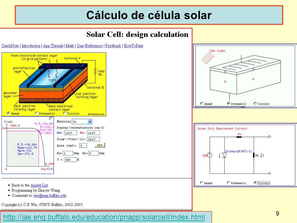
Cálculo de célula solar
10
Eficiência da célula solar
Como era considerado: Material Efficiency in lab (%) Efficiency of production cell (%) monocrystalline silicon about 24 14-17 polycrystalline silicon about 18 13-15 amorphous silicon about 13 5-7 É um tema atual, pode-se dizer que existe até publicações indicando até 100% de eficiência? The material is comprised of a hybrid of plastics, molybdenum and titanium. Outro:
 Efficiency of production cell (%) monocrystalline silicon. about polycrystalline silicon. about amorphous silicon. about É um tema atual, pode-se dizer que existe até publicações indicando até 100% de eficiência The material is comprised of a hybrid of plastics, molybdenum and titanium. Outro:")
11
Eficiência de células solares

12
Será que parou nos ~40% de eficiência?
New Solar Cell Technology Greatly Boosts Efficiency ScienceDaily (Apr. 29, 2011) — With the creation of a 3-D nanocone-based solar cell platform, a team led by Oak Ridge National Laboratory's Jun Xu has boosted the light-to-power conversion efficiency of photovoltaics by nearly 80 percent. The technology substantially overcomes the problem of poor transport of charges generated by solar photons. These charges -- negative electrons and positive holes -- typically become trapped by defects in bulk materials and their interfaces and degrade performance. "To solve the entrapment problems that reduce solar cell efficiency, we created a nanocone-based solar cell, invented methods to synthesize these cells and demonstrated improved charge collection efficiency," said Xu, a member of ORNL's Chemical Sciences Division. The new solar structure consists of n-type nanocones surrounded by a p-type semiconductor. The n-type nanoncones are made of zinc oxide and serve as the junction framework and the electron conductor. The p-type matrix is made of polycrystalline cadmium telluride and serves as the primary photon absorber medium and hole conductor. With this approach at the laboratory scale, Xu and colleagues were able to obtain a light-to-power conversion efficiency of 3.2 percent compared to 1.8 percent efficiency of conventional planar structure of the same materials. "We designed the three-dimensional structure to provide an intrinsic electric field distribution that promotes efficient charge transport and high efficiency in converting energy from sunlight into electricity," Xu said. Key features of the solar material include its unique electric field distribution that achieves efficient charge transport; the synthesis of nanocones using inexpensive proprietary methods; and the minimization of defects and voids in semiconductors. The latter provides enhanced electric and optical properties for conversion of solar photons to electricity. Because of efficient charge transport, the new solar cell can tolerate defective materials and reduce cost in fabricating next-generation solar cells. "The important concept behind our invention is that the nanocone shape generates a high electric field in the vicinity of the tip junction, effectively separating, injecting and collecting minority carriers, resulting in a higher efficiency than that of a conventional planar cell made with the same materials," Xu said. Research that forms the foundation of this technology was accepted by this year's Institute of Electrical and Electronics Engineers photovoltaic specialist conference and will be published in the IEEE Proceedings. The papers are titled "Efficient Charge Transport in Nanocone Tip-Film Solar Cells" and "Nanojunction solar cells based on polycrystalline CdTe films grown on ZnO nanocones." The research was supported by the Laboratory Directed Research and Development program and the Department of Energy's Office of Nonproliferation Research and Engineering. Other contributors to this technology are Sang Hyun Lee, X-G Zhang, Chad Parish, Barton Smith, Yongning He, Chad Duty and Ho Nyung Lee.
 — With the creation of a 3-D nanocone-based solar cell platform, a team led by Oak Ridge National Laboratory s Jun Xu has boosted the light-to-power conversion efficiency of photovoltaics by nearly 80 percent. The technology substantially overcomes the problem of poor transport of charges generated by solar photons. These charges -- negative electrons and positive holes -- typically become trapped by defects in bulk materials and their interfaces and degrade performance. To solve the entrapment problems that reduce solar cell efficiency, we created a nanocone-based solar cell, invented methods to synthesize these cells and demonstrated improved charge collection efficiency, said Xu, a member of ORNL s Chemical Sciences Division. The new solar structure consists of n-type nanocones surrounded by a p-type semiconductor. The n-type nanoncones are made of zinc oxide and serve as the junction framework and the electron conductor. The p-type matrix is made of polycrystalline cadmium telluride and serves as the primary photon absorber medium and hole conductor. With this approach at the laboratory scale, Xu and colleagues were able to obtain a light-to-power conversion efficiency of 3.2 percent compared to 1.8 percent efficiency of conventional planar structure of the same materials. We designed the three-dimensional structure to provide an intrinsic electric field distribution that promotes efficient charge transport and high efficiency in converting energy from sunlight into electricity, Xu said. Key features of the solar material include its unique electric field distribution that achieves efficient charge transport; the synthesis of nanocones using inexpensive proprietary methods; and the minimization of defects and voids in semiconductors. The latter provides enhanced electric and optical properties for conversion of solar photons to electricity. Because of efficient charge transport, the new solar cell can tolerate defective materials and reduce cost in fabricating next-generation solar cells. The important concept behind our invention is that the nanocone shape generates a high electric field in the vicinity of the tip junction, effectively separating, injecting and collecting minority carriers, resulting in a higher efficiency than that of a conventional planar cell made with the same materials, Xu said. Research that forms the foundation of this technology was accepted by this year s Institute of Electrical and Electronics Engineers photovoltaic specialist conference and will be published in the IEEE Proceedings. The papers are titled Efficient Charge Transport in Nanocone Tip-Film Solar Cells and Nanojunction solar cells based on polycrystalline CdTe films grown on ZnO nanocones. The research was supported by the Laboratory Directed Research and Development program and the Department of Energy s Office of Nonproliferation Research and Engineering. Other contributors to this technology are Sang Hyun Lee, X-G Zhang, Chad Parish, Barton Smith, Yongning He, Chad Duty and Ho Nyung Lee.")
13
Outros detectores

15
Superfícies fotoemissivas de PMT’s

16
Multiplicador de elétrons ou channeltron
A channeltron is effectively a photomultiplier with an infinite number of dynodes. It consists of a hollow, evacuated tube (the 'channel'), generally curved, of a few mm section and a few cm long, made of semiconducting glass: its inner surface acts as both, the photocathode and a continuous dynode. Channeltrons are used to detect optical, UV, X-ray light, electrons and ions (e.g. they were used as X-ray detectors on the Copernicus satellite, and in early MSSL magnetospheric experiments). Basically, when light, or charged particles, strike the channeltron's inner surface close to the entrance, electrons are expelled from it. An electric field, established by applying a positive voltage of several kV between the ends of the tube, accelerates the secondary electrons emitted at each point, they hit the walls again and again generating more and more secondary electrons; finally, the cloud of electrons is collected at the anode. The channeltron is curved to prevent 'ion feedback': this takes place when residual gas molecules, still present even if the device is run in vacuum, are ionised, becoming positive ions, are accelerated opposite to the electrons, reach the front end and release electrons which may produce spurious signals.
, generally curved, of a few mm section and a few cm long, made of semiconducting glass: its inner surface acts as both, the photocathode and a continuous dynode. Channeltrons are used to detect optical, UV, X-ray light, electrons and ions (e.g. they were used as X-ray detectors on the Copernicus satellite, and in early MSSL magnetospheric experiments). Basically, when light, or charged particles, strike the channeltron s inner surface close to the entrance, electrons are expelled from it. An electric field, established by applying a positive voltage of several kV between the ends of the tube, accelerates the secondary electrons emitted at each point, they hit the walls again and again generating more and more secondary electrons; finally, the cloud of electrons is collected at the anode. The channeltron is curved to prevent ion feedback : this takes place when residual gas molecules, still present even if the device is run in vacuum, are ionised, becoming positive ions, are accelerated opposite to the electrons, reach the front end and release electrons which may produce spurious signals.")
17
channeltron Voltagem de entrada V Defletores V

18
http://www. olympusmicro
19
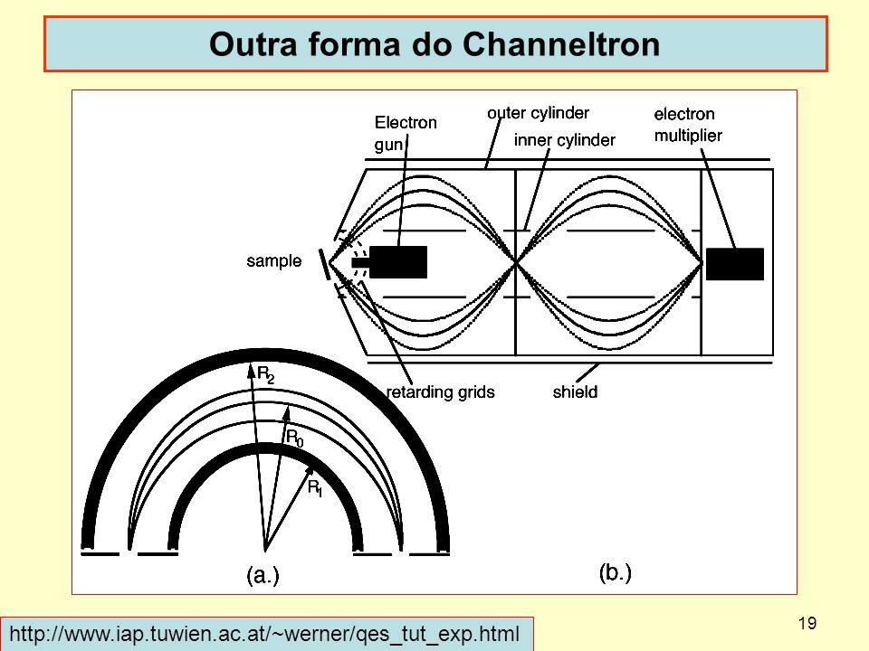
Outra forma do Channeltron
20
E a superfície para emissão?
Microchanneltron? Shown below is a cross section of the active surface of a Channeltron detector. Secondary emission occurs within the first 200 angstrom of the surface. Below this is a conductive layer that can be several thousands of angstrom thick. Surface & Plasma Technology Research Group of the Institut für Allgemeine Physik A variety of x-ray light sources is used in XPS studies, comprising the standard MgKα/AlKα twin anode laboratory source (shown in the Figure), (monochromated) rotating anode sources, UV lamps, or synchrotron light sources. The standard laboratory source shown in the Figure contains an Al/Mg twin-anode which is bombarded by electrons emitted from a filament that is held at ground potential. The anode is positively biased at ~15keV, in this way accelerating nearby electrons towards it. These electrons produce core holes in the anode target materials by electron impact ionization. The vacancies can relax by emission of characteristic x-rays that illuminate the sample. By switching the filament, AlKα (Ex=1485eV, ΔEFWHM= 0.85eV) or MgKα (Ex=1254eV, ΔEFWHM= 0.7eV). The observed line width is a consequence of the different x-ray lines contributing. For most line sources like the one shown in the Figure, the emission of Bremsstrahlung together with the desired characteristic x-ray line cannot be avoided and produces a broad (but weak) background in the spectrum. A thin Al-window prevents secondary and backscattered electrons to reach the sample. Since considerable power is dissipated in the anode ( W), the anode needs to be water cooled and must therefore be a good heat conductor (e.g. a metal). The anode top is silver coated to prevent Cu x-rays ghost lines from complicating the spectra when the anode material gets thin in the course of time. For high resolution studies of chemical states the quoted linewidths of the exciting radiation of ~1eV are sometimes prohibitively large. In such cases, monochromatized sources must be used. One way to achieve monochromatization of x-rays is to disperse the x-ray spectrum in a diffraction grating (a crystal). Since selection of a small energy band in a monochromator implies discarding a considerable fraction of the x-ray intensity, the anode must be operated at high power. Thus, cooling becomes a critical issue. For this reason, rotating anode x-ray sources are used in monochromated laboratory x-ray sources. The laboratory x-ray sources adressed above emit photons at a fixed energy. Very often it is desirable to be able to tune the energy of the incident light in a photoelectron emission experiment. The most convenient way to produce light with frequencies tunable over a certain range is to use an intense source with a broad continuous spectrum and employing a monochromator to select the desired frequency. Such a source is realized in a synchrotron for energies between UV and hard x-rays (~30keV). When a charged particle in a storage ring is deflected (accelerated) to maintain its trajectory within the torus, it emits Bremsstrahlung. This process is particularly effective for electrons owing to their small resting mass. In a synchrotron, electrons are accelerated to velocities approaching the speed of light, and an intense Bremsstrahlungsspectrum is emitted. It extends down in energy to the UV-regime, while the intensity falls off rapidly above a maximum energy determined by the critical energy of the synchrotron-a design parameter. The emitted spectrum is highly collimated to within a fraction of a mrad along the tangential direction of the torus. Therefore such a light beam is ideally suited for monochromatization. Indeed, the intensity of photon beams (after monochromatization) produced in this way may exceed those of laboratory sources by up to 10 orders of magnitude. Furthermore, different polarization states of the light can be produced (linear polarization near the center of the beam in the central plane of the torus, circular polarization off-plane). Another useful feature of synchrotron light is that it is produced by bunches of electrons orbiting the torus (bunch duration~100ps) and therefore the light has a well defined time structure that can be advantageous in e.g. coincidence experiments. Common electron guns in electron spectroscopy can produce a beam of medium energy electrons (~50eV-50keV) with a beam current of typically some nanoamperes and an energy spread less than an eV. The two most popular types of electron guns are the thermionic emission gun (shown schematically in the figure) and the field emission gun. In thermionic emission the mean energy of the electron gas in the solid is increased by resistively heating the filament providing a certain fraction of the loosely bound electrons with an energy exceeding the work function barrier. The cathode material in this case must have a high melting point and a possibly low work function. These requirements are met by Tungsten that is often used as filament. Thoria coated metals as well as LaB6 single crystals have still a lower work function and are also used. At the core of each apparatus for electron spectrometry is a component that performs the actual selection of the electron energy or speed. The most common analyzers in use today are electrostatic analyzers: the cylindrical mirror analyzer (CMA) and the hemispherical mirror analyzer (HMA) that is sometimes referred to as concentrical hemispherical analyzer (CHA). The retarding field analyzer (RFA) that is employed to acquire low energy electron diffraction data is sometimes also used for Auger electron spectroscopy, mainly for qualitative purposes of checking sample cleanliness but is not optimally suited for electron spectroscopy in general. The Figure schematically shows the CHA and CMA type analyzers. In a CHA, an electrostatic field is applied between an inner and outer hemisphere Electrons with an energy equal to the pass energy that are injected through the entrance slit tangentially to the median hemispherical surface are transferred from the entrance slit to the detector. They then describe a circular trajectory on the median hemispherical surface The potential difference between the hemispheres determines the pass energy. The energy resolution of the CHA is determined by the radius and the width of the slits at the analyzer entrance and exit. A lens is used to transfer electrons from the sample to the entrance slit. The electron optics in the transfer lens assembly also contain an element that retards or accelerates electrons of a given energy to the pass energy. The polar opening angle $\Delta\alpha$ is of the order of several degrees and the solid angle is therefore rather small. For example for a 12° full polar opening angle the solid angle is approximately ΔΩ= 2πxcos 12 °=0.01 x 4 π. Therefore the best attainable transmission of such an analyzer would be ~1%. The analyzer shown schematically in panel b of the figure is a double pass CMA. It consists of two concentric cylinders. The inner cylinder is held at ground potential while the outer cylinder is at a certain negative potential. The electric field between the cylinders forces the electrons entering it to describe trajectories with a radius depending on their energy and the field in the analyzer. Only those electrons with a given energy, the so-called pass energy, are focussed onto the electron detector and are registered by the acquisition electronics. The entrance aperture of the CMA is annular in shape.The aperture is usually located at a polar angle of θa=42°.15'.5''. For this special geometry a second order focus is formed at the exit slit of each stage of the analyzer. In this case the pass energy is related to the potential V at the outer cylinder and the radii of the cylinders. The (half polar) angular width of the annulus can be made as wide as Δα=6° without noticeably deteriorating the energy resolution. Therefore, the solid angle of acceptance of a CMA is quite large, ΔΩ~ 2π(cos 36-cos 48)=0.14 x 4π. In consequence, the transmission of a CMA is relatively high and would optimally amount to ~14%. This may constitute a major advantage over the CHA if sensitivity is a critical issue. Two drawbacks of the CMA should be mentioned: the intensity as well as the energy calibration depend strongly on the sample analyzer distance making very careful adjustment of the sample necessary. This poses significant geometrical limitations to an apparatus containing a CMA for energy selection: while in the case of a CHA a lens can be used to transfer the signal electrons to the spectrometer entrance so that the distance between the analyzer and the sample can be of the order of some tens of cm, this is strictly impossible in the case of the CMA. Recording of an electron energy spectrum, i.e. the energy distribution of particles leaving the specimen, can be performed in two modes, the so-called constant analyzer energy (CAE) and constant retard ratio (CRR) mode. In the CAE mode, the electric field in the analyzer, and thus the analyzer pass energy, is kept constant, and a variable retarding voltage is applied to retardation grids (or the decelaration element in the transfer lens of a CHA). In this way, only electrons that leave the target with an energy E can pass through the analyzer before they are detected. By recording the number of detected electrons as a function of the retarding voltage the electron spectrum is obtained. Alternatively, an electron energy distribution may be obtained by variation of the pass energy, keeping the ratio between the pass energy and the retardation voltage constant. This is done in the CRR mode. Since the spatial divergence of the electron trajectories in the analyzer increases with decreasing pass energy, the energy resolution in the CRR mode is proportional to the detected energy Δ E α E, whereas in the CAE mode the energy resolution is constant over the entire spectrum. The CAE mode is therefore usually used in XPS since a constant energy resolution over the entire spectrum is desirable in this case. For AES, on the other hand, energy resolution of the spectrometer is not crucial since the Auger peaks generally exhibit a rather large intrinsic linewidth of >1eV. Furthermore, for electron excited AES, the peaks are superimposed on a broad and intense background of inelastically backscattered primary electrons rising monotonically with kinetic energy. Therefore, the important issue in electron excited AES is the signal to background ratio being important for the sensitivity rather than energy resolution. Then it is advantageous to operate the spectrometer in the CRR mode. Generally, when electron excited AES uses fine focussed electron beams to perform nanoanalysis, the signal may originate only from a very small volume. This again emphasizes the importance of high transmission spectrometers for AES. Since furthermore neither energy nor angular resolution is essential in most applications, a CMA is commonly used for AES. Recently, however, CHAs with special transfer lens systems have become available for which the transmission is comparable to that of the CMA. For XPS, the situation is just the opposite: usually a good energy resolution is crucial, sometimes angular resolution is desired, but sensitivity is much less an issue than in AES since the area of the sample from which the signal electrons originate is always rather large while the signal to background ratio is almost always much better than for electron excited AES where the background of inelastically backscattered primaries dominates the entire spectrum. A channeltron, shown in panel a of the figure is often used as electron detector. This is a bent tube that is coated with an insulator with a high secondary electron coefficient. Over this tube, a potential of about 2.5kV is applied. When an electron strikes the mouth of the tube, a number of secondaries is produced that is accelerated in the channeltron. These accelerated secondaries in turn produce secondaries and so on. In effect, a large number of secondaries is produced. The energy required to produce these secondaries is supplied by the channeltron voltage supply. In this way a pulse is produced that indicates the arrival of an electron in the detector. This pulse is then shaped and ultimately registered by the acquisition electronics. In a similar way, pulses of electrons are produced in the microchannels of a microchannel plate (MCP) (panel b) When this device is used in combination with a position sensitive anode, electrons can be detected with a lateral resolution of some tens of a micron. In view of the high surface sensitivity of techniques like AES, it is necessary to conduct experiments at low ambient pressures (UHV, ultra high vacuum p~ mbar) in order to avoid contamination of the surface under study by absorption of ambient atoms or molecules. Ambient pressures in this range can be attained routinely in a modern UHV system. Such a system generally consists of a stainless steel vessel to which all the required components are attached through flanges that are leak sealed by means of copper gaskets. The apparatus must be evacuated down to the desired pressure by a system of pumps. Since the walls of the apparatus are always covered with water vapour when the system has been to air and the desorption of this vapour is a very slow process (of the order of weeks at room temperature), the entire system must be baked to above the boiling point of water overnight. Monitoring of the pressure is performed by means of various pressure gauges and sometimes a quadrupole mass spectrometer is used to study the composition of the resiudual gas in detail. The Figure shows the pressure ranges in which the different types of pumps and pressure gauges can be operated. Contents » E a superfície para emissão?
, (monochromated) rotating anode sources, UV lamps, or synchrotron light sources. The standard laboratory source shown in the Figure contains an Al/Mg twin-anode which is bombarded by electrons emitted from a filament that is held at ground potential. The anode is positively biased at ~15keV, in this way accelerating nearby electrons towards it. These electrons produce core holes in the anode target materials by electron impact ionization. The vacancies can relax by emission of characteristic x-rays that illuminate the sample. By switching the filament, AlKα (Ex=1485eV, ΔEFWHM= 0.85eV) or MgKα (Ex=1254eV, ΔEFWHM= 0.7eV). The observed line width is a consequence of the different x-ray lines contributing. For most line sources like the one shown in the Figure, the emission of Bremsstrahlung together with the desired characteristic x-ray line cannot be avoided and produces a broad (but weak) background in the spectrum. A thin Al-window prevents secondary and backscattered electrons to reach the sample. Since considerable power is dissipated in the anode ( W), the anode needs to be water cooled and must therefore be a good heat conductor (e.g. a metal). The anode top is silver coated to prevent Cu x-rays ghost lines from complicating the spectra when the anode material gets thin in the course of time. For high resolution studies of chemical states the quoted linewidths of the exciting radiation of ~1eV are sometimes prohibitively large. In such cases, monochromatized sources must be used. One way to achieve monochromatization of x-rays is to disperse the x-ray spectrum in a diffraction grating (a crystal). Since selection of a small energy band in a monochromator implies discarding a considerable fraction of the x-ray intensity, the anode must be operated at high power. Thus, cooling becomes a critical issue. For this reason, rotating anode x-ray sources are used in monochromated laboratory x-ray sources. The laboratory x-ray sources adressed above emit photons at a fixed energy. Very often it is desirable to be able to tune the energy of the incident light in a photoelectron emission experiment. The most convenient way to produce light with frequencies tunable over a certain range is to use an intense source with a broad continuous spectrum and employing a monochromator to select the desired frequency. Such a source is realized in a synchrotron for energies between UV and hard x-rays (~30keV). When a charged particle in a storage ring is deflected (accelerated) to maintain its trajectory within the torus, it emits Bremsstrahlung. This process is particularly effective for electrons owing to their small resting mass. In a synchrotron, electrons are accelerated to velocities approaching the speed of light, and an intense Bremsstrahlungsspectrum is emitted. It extends down in energy to the UV-regime, while the intensity falls off rapidly above a maximum energy determined by the critical energy of the synchrotron-a design parameter. The emitted spectrum is highly collimated to within a fraction of a mrad along the tangential direction of the torus. Therefore such a light beam is ideally suited for monochromatization. Indeed, the intensity of photon beams (after monochromatization) produced in this way may exceed those of laboratory sources by up to 10 orders of magnitude. Furthermore, different polarization states of the light can be produced (linear polarization near the center of the beam in the central plane of the torus, circular polarization off-plane). Another useful feature of synchrotron light is that it is produced by bunches of electrons orbiting the torus (bunch duration~100ps) and therefore the light has a well defined time structure that can be advantageous in e.g. coincidence experiments. Common electron guns in electron spectroscopy can produce a beam of medium energy electrons (~50eV-50keV) with a beam current of typically some nanoamperes and an energy spread less than an eV. The two most popular types of electron guns are the thermionic emission gun (shown schematically in the figure) and the field emission gun. In thermionic emission the mean energy of the electron gas in the solid is increased by resistively heating the filament providing a certain fraction of the loosely bound electrons with an energy exceeding the work function barrier. The cathode material in this case must have a high melting point and a possibly low work function. These requirements are met by Tungsten that is often used as filament. Thoria coated metals as well as LaB6 single crystals have still a lower work function and are also used. At the core of each apparatus for electron spectrometry is a component that performs the actual selection of the electron energy or speed. The most common analyzers in use today are electrostatic analyzers: the cylindrical mirror analyzer (CMA) and the hemispherical mirror analyzer (HMA) that is sometimes referred to as concentrical hemispherical analyzer (CHA). The retarding field analyzer (RFA) that is employed to acquire low energy electron diffraction data is sometimes also used for Auger electron spectroscopy, mainly for qualitative purposes of checking sample cleanliness but is not optimally suited for electron spectroscopy in general. The Figure schematically shows the CHA and CMA type analyzers. In a CHA, an electrostatic field is applied between an inner and outer hemisphere Electrons with an energy equal to the pass energy that are injected through the entrance slit tangentially to the median hemispherical surface are transferred from the entrance slit to the detector. They then describe a circular trajectory on the median hemispherical surface The potential difference between the hemispheres determines the pass energy. The energy resolution of the CHA is determined by the radius and the width of the slits at the analyzer entrance and exit. A lens is used to transfer electrons from the sample to the entrance slit. The electron optics in the transfer lens assembly also contain an element that retards or accelerates electrons of a given energy to the pass energy. The polar opening angle $\Delta\alpha$ is of the order of several degrees and the solid angle is therefore rather small. For example for a 12° full polar opening angle the solid angle is approximately ΔΩ= 2πxcos 12 °=0.01 x 4 π. Therefore the best attainable transmission of such an analyzer would be ~1%. The analyzer shown schematically in panel b of the figure is a double pass CMA. It consists of two concentric cylinders. The inner cylinder is held at ground potential while the outer cylinder is at a certain negative potential. The electric field between the cylinders forces the electrons entering it to describe trajectories with a radius depending on their energy and the field in the analyzer. Only those electrons with a given energy, the so-called pass energy, are focussed onto the electron detector and are registered by the acquisition electronics. The entrance aperture of the CMA is annular in shape.The aperture is usually located at a polar angle of θa=42° For this special geometry a second order focus is formed at the exit slit of each stage of the analyzer. In this case the pass energy is related to the potential V at the outer cylinder and the radii of the cylinders. The (half polar) angular width of the annulus can be made as wide as Δα=6° without noticeably deteriorating the energy resolution. Therefore, the solid angle of acceptance of a CMA is quite large, ΔΩ~ 2π(cos 36-cos 48)=0.14 x 4π. In consequence, the transmission of a CMA is relatively high and would optimally amount to ~14%. This may constitute a major advantage over the CHA if sensitivity is a critical issue. Two drawbacks of the CMA should be mentioned: the intensity as well as the energy calibration depend strongly on the sample analyzer distance making very careful adjustment of the sample necessary. This poses significant geometrical limitations to an apparatus containing a CMA for energy selection: while in the case of a CHA a lens can be used to transfer the signal electrons to the spectrometer entrance so that the distance between the analyzer and the sample can be of the order of some tens of cm, this is strictly impossible in the case of the CMA. Recording of an electron energy spectrum, i.e. the energy distribution of particles leaving the specimen, can be performed in two modes, the so-called constant analyzer energy (CAE) and constant retard ratio (CRR) mode. In the CAE mode, the electric field in the analyzer, and thus the analyzer pass energy, is kept constant, and a variable retarding voltage is applied to retardation grids (or the decelaration element in the transfer lens of a CHA). In this way, only electrons that leave the target with an energy E can pass through the analyzer before they are detected. By recording the number of detected electrons as a function of the retarding voltage the electron spectrum is obtained. Alternatively, an electron energy distribution may be obtained by variation of the pass energy, keeping the ratio between the pass energy and the retardation voltage constant. This is done in the CRR mode. Since the spatial divergence of the electron trajectories in the analyzer increases with decreasing pass energy, the energy resolution in the CRR mode is proportional to the detected energy Δ E α E, whereas in the CAE mode the energy resolution is constant over the entire spectrum. The CAE mode is therefore usually used in XPS since a constant energy resolution over the entire spectrum is desirable in this case. For AES, on the other hand, energy resolution of the spectrometer is not crucial since the Auger peaks generally exhibit a rather large intrinsic linewidth of >1eV. Furthermore, for electron excited AES, the peaks are superimposed on a broad and intense background of inelastically backscattered primary electrons rising monotonically with kinetic energy. Therefore, the important issue in electron excited AES is the signal to background ratio being important for the sensitivity rather than energy resolution. Then it is advantageous to operate the spectrometer in the CRR mode. Generally, when electron excited AES uses fine focussed electron beams to perform nanoanalysis, the signal may originate only from a very small volume. This again emphasizes the importance of high transmission spectrometers for AES. Since furthermore neither energy nor angular resolution is essential in most applications, a CMA is commonly used for AES. Recently, however, CHAs with special transfer lens systems have become available for which the transmission is comparable to that of the CMA. For XPS, the situation is just the opposite: usually a good energy resolution is crucial, sometimes angular resolution is desired, but sensitivity is much less an issue than in AES since the area of the sample from which the signal electrons originate is always rather large while the signal to background ratio is almost always much better than for electron excited AES where the background of inelastically backscattered primaries dominates the entire spectrum. A channeltron, shown in panel a of the figure is often used as electron detector. This is a bent tube that is coated with an insulator with a high secondary electron coefficient. Over this tube, a potential of about 2.5kV is applied. When an electron strikes the mouth of the tube, a number of secondaries is produced that is accelerated in the channeltron. These accelerated secondaries in turn produce secondaries and so on. In effect, a large number of secondaries is produced. The energy required to produce these secondaries is supplied by the channeltron voltage supply. In this way a pulse is produced that indicates the arrival of an electron in the detector. This pulse is then shaped and ultimately registered by the acquisition electronics. In a similar way, pulses of electrons are produced in the microchannels of a microchannel plate (MCP) (panel b) When this device is used in combination with a position sensitive anode, electrons can be detected with a lateral resolution of some tens of a micron. In view of the high surface sensitivity of techniques like AES, it is necessary to conduct experiments at low ambient pressures (UHV, ultra high vacuum p~ mbar) in order to avoid contamination of the surface under study by absorption of ambient atoms or molecules. Ambient pressures in this range can be attained routinely in a modern UHV system. Such a system generally consists of a stainless steel vessel to which all the required components are attached through flanges that are leak sealed by means of copper gaskets. The apparatus must be evacuated down to the desired pressure by a system of pumps. Since the walls of the apparatus are always covered with water vapour when the system has been to air and the desorption of this vapour is a very slow process (of the order of weeks at room temperature), the entire system must be baked to above the boiling point of water overnight. Monitoring of the pressure is performed by means of various pressure gauges and sometimes a quadrupole mass spectrometer is used to study the composition of the resiudual gas in detail. The Figure shows the pressure ranges in which the different types of pumps and pressure gauges can be operated. Contents » E a superfície para emissão")
21
channeltron

22
Aplicação?

24
Aplicação

25
Aplicação? Visão noturna E.I.T. = Enhanced Image Tube

26
Com raios-X Modo Espectral
– Área analisada de 2x1mm até 15 mícrons de diâmetro. –energia: 5 to 160 eV –8 channeltron multi-detector

27
Fotocondutividade Processo para fotocondutividade intrínseca: fotoexcitação provoca geração de portadores de carga que vão para a banda de condução. Desde que exista uma ddp aplicada, permite a mudança de corrente sobre o efeito da luz. Para o caso extrínseco, portador de carga doador pode ser excitado para banda de condução, aumentando a condutividade, como tb pode ocorrer a criação de buracos com a excitação de elétrons para o nível aceitador.

28
Detectores fotocondutivos intrínsecos

29
Detector fotocondutivo
Tempo de vida do portador # de portadores em excesso gerados pela luz Função degrau Solução td é o tempo que o portador atravessa o gap (d) provocando uma corrente q/ td. i é a corr. externa
 provocando uma corrente q/ td. i é a corr. externa.")
30
Detectores PIN e APD Detectores térmicos Fotoacústicos

31
Detectores usados em fibras ópticas
PIN diode ou diodo PIN (P Intrinsic N). O diodo PIN possui uma camada intrínseca entre as camadas P e N de um diodo. APD (Avalanche PhotoDiode) ou fotodiodo de avalanche. Mais sensível que o fotodiodo pin
. O diodo PIN possui uma camada intrínseca entre as camadas P e N de um diodo. APD (Avalanche PhotoDiode) ou fotodiodo de avalanche. Mais sensível que o fotodiodo pin.")
32
Fotodiodo pn (a) e fotodiodo pin (b)
Circuito equivalente

34
Fotodiodo pin A camada intrínseca serve para aumentar a região da junção, conseqüentemente melhora a fotoconversão. Modo fotovoltaico qdo não há campo externo Modo fotocondutor qdo polarizado por fonte externa

35
Resposta espectral fotodiodo pin de Si
Responsividade típica R A – REALÇADO PARA 900nm B – REALÇADO PARA 1060nm Destaque para algumas fontes emissivas

36
Fotodiodo avalanche (APD)
A desvantagem de um fotodiodo pin produzir apenas um par de portadores de carga. No APD uma ddp aplicada de forma reversa de até 2kV acelera os fotoelétrons de maneira que cada fotoelétron primário resulta em milhares de elétrons no eletrodo.

37
http://micro. magnet. fsu
Ver arquivo APDFinalPaper.doc

38
PIN e APD Tabela 1 – Comparação de fotodiodo PIN e APDs Parametro PIN
Tipo de material Si, Ge, InGaAs Largura de banda DC a 40+ GHz Comprimento de onda 0.6 to 1.8 µm Eficiência de conversão 0.5 to 1.0 Amps/Watt 0.5 to 100 Amps/Watt Circuito eletrônico de apoio Não precisa Alta tensão, temperatura estabilizada Custos (pronto para fibra) $1 to $500 $100 to $2,000
 $1 to $500. $100 to $2,000.")
39
Sem esquecer o fototransistor
Photo Transistor: One of the most popular light detectors is the photo transistor. They are cheap, readily available and have been used in many published communications circuits. But as I have indicated above, the PIN photodiode is still a much better choice if you want systems with better performance. As shown in Figure 2b-1, a phototransistor is a silicon photodiode connected to the base-emitter terminals of a silicon transistor. Since the phototransistor it is made of silicon, it has a similar response curve as a standard silicon PIN photodiode. Figure 2b-1The photodiode is connected directly to the transistor, it is not reversed biased and operates in a photovoltaic mode. The current produced by the photodiode is routed to the transistor that provides a sizable current gain. This amplification gives the photo transistor much more light sensitivity than a standard PIN diode. But, with the gain comes a price. The photodiode/transistor connection dramatically slows down the otherwise fast response time of the diode inside. Most phototransistors will have response times measured in tens of microseconds, which is some 100 times slower than similar PIN diodes. Such slow speeds reduce the usefulness of the device in most communications systems. They also have the disadvantage of having small active areas and high noise levels. You will often find them being used for simple light reflector and detector applications that do not rely on fast light pulses. But, overall, they are a poor substitute for a good PIN diode when connected to well designed receiver circuit. Prático, mas convêm ainda o APD

40
Como aumentar a absorção de luz do detector?
Aumentar a sensitividade do detector com filmes anti-refletores. Criar armadilhas de fótons através de bobinas de nano-fios refrigerados THeL. Aumento de fótons armadilhados => aumento na eficiência de conversão.

41
Detectores térmicos Termopar Piroelétrico Bolômetro

42
Origem do termopar Efeito Seebeck Thomas Johann Seebeck (1770-1831)
Profissão Descoberta – bússola Também denominado de efeito termoelétrico. Existem outros efeitos termoelétricos.

43
Efeitos termoelétricos
Ocorre quando portadores de carga moveis estão sujeitos à influencia de gradientes de temperatura e/ou gradientes de potencial elétrico. Na ausência de um campo magnético existem três tipos de efeitos termoelétricos. Efeito Seebeck Efeito Peltier Efeito Thomson Thomson effect One of three reversible thermoelectric phenomena (often known simply as thermoelectric effects), the others being the Seebeck effect and a Peltier effect. In 1851 William Thomson (later Lord Kelvin) was led by thermodynamic reasoning to conclude that sources of electromotive force (emf) exist in a thermoelectric circuit in addition to those located at the junctions. In particular, he predicted that an emf would arise within in a single conductor whenever a temperature gradient was present. The truth of this prediction can be demonstrated by the experiment illustrated in the diagram here. In this experiment a current passes through an iron rod which is bent into a U-shape. Resistance coils, R1 and R2, are wound about the two sides of the U, as shown. These form two arms of a balanced Wheatstone bridge. The bottom of the U is then heated. This establishes two temperature gradients – a positive one extending from A to C, and a negative one extending from C to B. As a result of this operation, the bridge becomes in such a direction as to indicate that the resistance of R1 has increased more than that of R2. Evidently, heat has been liberated R1 and absorbed at R2. Absorption of heat is evidence for an electromotive force (emf) that is acting in the same direction as that of the current, that is to say, electrical energy is being supplied to the circuit at the expense of heat energy of the environment. Such is the case in the section. Likewise, in the section AC, the current is opposed by an emf, with consequent transformation of electrical energy into heat energy. Thus, in iron, the Thomson emf would would give rise to a current in the iron from hot to cold regions. many metals, including bismuth, cobalt, nickel, and platinum, in addition to iron, exhibit this same property, which is referred to as the negative Thomson effect. Another group of metals, including antimony, cadmium, copper, and silver, display a positive Thomson effect; in these, the direction of the Thomson emf is such as to support a current within the metal from cold to hot regions. In one metal, lead, the Thomson effect is zero. In certain metals the effect reverses sign as the temperature is raised or as the crystal structure is altered. The magnitude of the Thomson emf for a given material, a, is expressed in terms of the Thomson coefficient, σa, which has dimensions of emf/degree. Thus σa dt is the emf that exists between two points whose temperatures differ by dt °C. Hence, the heat absorbed per second between two points at temperature t1 and t2, respectively, when a current of I amperes passes through the material, is given by Heat absorbed/sec = I [integral between t1 and t2]σa dt - I2R The Thomson coefficient, σa, is positive (negative) for materials exhibiting the positive (negative) Thomson effect. The term in the equation above is simply the Joule heat that is always liberated when a current flows through an imperfect conductor. It has no relation to the Thomson effect, but is included in the equation for completeness. It appears that the total Thomson emf along a conductor depends only upon the temperatures of the two ends, and not in any way upon the particular manner in which the temperature gradient varies. This empirically observed fact is known, after its discoverer, as the law of Malus (1851). In 1851 William Thomson (later Lord Kelvin) S.O. Kasap -Thermoelectric effects in metals
, the others being the Seebeck effect and a Peltier effect. In 1851 William Thomson (later Lord Kelvin) was led by thermodynamic reasoning to conclude that sources of electromotive force (emf) exist in a thermoelectric circuit in addition to those located at the junctions. In particular, he predicted that an emf would arise within in a single conductor whenever a temperature gradient was present. The truth of this prediction can be demonstrated by the experiment illustrated in the diagram here. In this experiment a current passes through an iron rod which is bent into a U-shape. Resistance coils, R1 and R2, are wound about the two sides of the U, as shown. These form two arms of a balanced Wheatstone bridge. The bottom of the U is then heated. This establishes two temperature gradients – a positive one extending from A to C, and a negative one extending from C to B. As a result of this operation, the bridge becomes in such a direction as to indicate that the resistance of R1 has increased more than that of R2. Evidently, heat has been liberated R1 and absorbed at R2. Absorption of heat is evidence for an electromotive force (emf) that is acting in the same direction as that of the current, that is to say, electrical energy is being supplied to the circuit at the expense of heat energy of the environment. Such is the case in the section. Likewise, in the section AC, the current is opposed by an emf, with consequent transformation of electrical energy into heat energy. Thus, in iron, the Thomson emf would would give rise to a current in the iron from hot to cold regions. many metals, including bismuth, cobalt, nickel, and platinum, in addition to iron, exhibit this same property, which is referred to as the negative Thomson effect. Another group of metals, including antimony, cadmium, copper, and silver, display a positive Thomson effect; in these, the direction of the Thomson emf is such as to support a current within the metal from cold to hot regions. In one metal, lead, the Thomson effect is zero. In certain metals the effect reverses sign as the temperature is raised or as the crystal structure is altered. The magnitude of the Thomson emf for a given material, a, is expressed in terms of the Thomson coefficient, σa, which has dimensions of emf/degree. Thus σa dt is the emf that exists between two points whose temperatures differ by dt °C. Hence, the heat absorbed per second between two points at temperature t1 and t2, respectively, when a current of I amperes passes through the material, is given by. Heat absorbed/sec = I [integral between t1 and t2]σa dt - I2R. The Thomson coefficient, σa, is positive (negative) for materials exhibiting the positive (negative) Thomson effect. The term in the equation above is simply the Joule heat that is always liberated when a current flows through an imperfect conductor. It has no relation to the Thomson effect, but is included in the equation for completeness. It appears that the total Thomson emf along a conductor depends only upon the temperatures of the two ends, and not in any way upon the particular manner in which the temperature gradient varies. This empirically observed fact is known, after its discoverer, as the law of Malus (1851). In 1851 William Thomson (later Lord Kelvin) S.O. Kasap -Thermoelectric effects in metals.")
44
Efeito Seebeck Uma diferença de temperatura entre dois pontos de um condutor ou de um semicondutor resulta numa ddp entre esses dois pontos. De outra forma: a gradiente de temperatura num condutor ou semicondutor da lugar a um campo elétrico. O coeficiente Seebeck calibra a magnitude desse efeito. A voltagem termoelétrica desenvolvida por unidade de diferença de temperatura num condutor é denominada de coeficiente Seebeck. Somente a ddp neto de Seebeck entre metais diferentes pode ser medido. O principio do termopar é baseado no efeito Seebeck. 1. The Seebeck Effect and Normal Metals Consider an aluminum rod that is heated at one end and cooled at the other end as depicted in Figure 1. The electrons in the hot region are more energetic and therefore have greater velocities than those in the cold region1. Consequently there is a net diffusion of electrons from the hot end toward the cold end which leaves behind exposed positive metal ions in the hot region and accumulates electrons in the cold region. This situation prevails until the electric field developed between the positive ions in the hot region and the excess electrons in the cold region prevents further electron motion from the hot to cold end. A voltage is therefore developed between the hot and cold ends with the hot end at positive potential.

45
Efeito Seebeck (Notes on using thermocouples - Dr. Robert J
Efeito Seebeck (Notes on using thermocouples - Dr. Robert J. Moffat, Stanford University) O coeficiente de Seebeck: Ferro-constantan (J) Cromel-alumel (K) Cobre-constantan (T) Outros Any two wires of different materials can be used as a thermocouple if connected together as in Figure 1. The AB connection is called the "junction". When the junction temperature, TJct, is different from the reference temperature, TRef, a low-level DC voltage, E , will be available at the +/- terminals. The value of E depends on the materials A and B, on the reference temperature, and on the junction temperature. The governing equations for two-wire thermocouples are shown in Eq. 1 through to Eq. 4. If a circuit has more than two wires, more terms would be needed. From Eq. 1, we can see that the EMF is generated by the wires, not the junction: the junction being just an electrical connection between the two wires. The signal is generated in the wires where the temperature gradient, dt/dx, is not zero: uniform temperature wires do not generate any EMF. If both wires are uniform in calibration, then Eq. 2 can be used, and if the two wires both begin at TRef and end at TJct, then Eq. 3 applies. EMF-Temperature tables can only be used when the circuit consists of only two wires, both of which are uniform in calibration, and both of which begin at TRef and end at TJct. When only small temperature differences are involved, the values of A and B can be treated as constants, and Eq. 4 gives a good approximation to the EMF.
 O coeficiente de Seebeck: Ferro-constantan (J) Cromel-alumel (K) Cobre-constantan (T) Outros. Any two wires of different materials can be used as a thermocouple if connected together as in Figure 1. The AB connection is called the junction . When the junction temperature, TJct, is different from the reference temperature, TRef, a low-level DC voltage, E , will be available at the +/- terminals. The value of E depends on the materials A and B, on the reference temperature, and on the junction temperature. The governing equations for two-wire thermocouples are shown in Eq. 1 through to Eq. 4. If a circuit has more than two wires, more terms would be needed. From Eq. 1, we can see that the EMF is generated by the wires, not the junction: the junction being just an electrical connection between the two wires. The signal is generated in the wires where the temperature gradient, dt/dx, is not zero: uniform temperature wires do not generate any EMF. If both wires are uniform in calibration, then Eq. 2 can be used, and if the two wires both begin at TRef and end at TJct, then Eq. 3 applies. EMF-Temperature tables can only be used when the circuit consists of only two wires, both of which are uniform in calibration, and both of which begin at TRef and end at TJct. When only small temperature differences are involved, the values of A and B can be treated as constants, and Eq. 4 gives a good approximation to the EMF.")
46
Efeito Peltier É o efeito reverso do Seebeck Metal Semicondutor
é o coeficiente de Peltier Refrigeração, uso doméstico, detectores The Peltier effect is the reverse of the Seebeck effect; a creation of a heat difference from an electric voltage. It occurs when a current is passed through two dissimilar metals or semiconductors (n-type and p-type) that are connected to each other at two junctions (Peltier junctions). The current drives a transfer of heat from one junction to the other: one junction cools off while the other heats up; as a result, the effect is often used for thermoelectric cooling. This effect was observed in 1834 by Jean Peltier, 13 years after Seebeck's initial discovery. When a current I is made to flow through the circuit, heat is evolved at the upper junction (at T2), and absorbed at the lower junction (at T1). The Peltier heat absorbed by the lower junction per unit time, is equal to Where Π is the Peltier coefficient ΠAB of the entire thermocouple, and ΠA and ΠB are the coefficients of each material. P-type silicon typically has a positive Peltier coefficient (though not above ~550 K), and n-type silicon is typically negative. The conductors are attempting to return to the electron equilibrium that existed before the current was applied by absorbing energy at one connector and releasing it at the other. The individual couples can be connected in series to enhance the effect. The direction of heat transfer is controlled by the polarity of the current; reversing the polarity will change the direction of transfer and thus the sign of the heat absorbed/evolved. A Peltier cooler/heater or thermoelectric heat pump is a solid-state active heat pump which transfers heat from one side of the device to the other. Peltier coolers are also called thermo-electric coolers (TEC).
 that are connected to each other at two junctions (Peltier junctions). The current drives a transfer of heat from one junction to the other: one junction cools off while the other heats up; as a result, the effect is often used for thermoelectric cooling. This effect was observed in 1834 by Jean Peltier, 13 years after Seebeck s initial discovery. When a current I is made to flow through the circuit, heat is evolved at the upper junction (at T2), and absorbed at the lower junction (at T1). The Peltier heat absorbed by the lower junction per unit time, is equal to. Where Π is the Peltier coefficient ΠAB of the entire thermocouple, and ΠA and ΠB are the coefficients of each material. P-type silicon typically has a positive Peltier coefficient (though not above ~550 K), and n-type silicon is typically negative. The conductors are attempting to return to the electron equilibrium that existed before the current was applied by absorbing energy at one connector and releasing it at the other. The individual couples can be connected in series to enhance the effect. The direction of heat transfer is controlled by the polarity of the current; reversing the polarity will change the direction of transfer and thus the sign of the heat absorbed/evolved. A Peltier cooler/heater or thermoelectric heat pump is a solid-state active heat pump which transfers heat from one side of the device to the other. Peltier coolers are also called thermo-electric coolers (TEC).")
47
Efeito Thomson – Lord Kelvin 1851
Descreve o aquecimento ou resfriamento de um condutor portador de carga com a gradiente de temperatura. r resistividade J densidade de corrente m coeficiente de Thomson(pode ser +-, depende do material) dT/dx gradiente de temperatura Thomson effect Thomson effect, named for William Thomson (Lord Kelvin), describes the heating or cooling of a current-carrying conductor with a temperature gradient. Any current-carrying conductor, with a temperature difference between two points, will either absorb or emit heat, depending on the material. If a current density J is passed through a homogeneous conductor, heat production per unit volume is where ρ is the resistivity of the material dT/dx is the temperature gradient along the wire μ is the Thompson coefficient. The first term ρ J is simply the Joule heating, which is not reversible. The second term is the Thomson heat, which changes sign when J changes directions. The Peltier and Seebeck coefficients are related by the Thomson relation
 dT/dx gradiente de temperatura. Thomson effect. Thomson effect, named for William Thomson (Lord Kelvin), describes the heating or cooling of a current-carrying conductor with a temperature gradient. Any current-carrying conductor, with a temperature difference between two points, will either absorb or emit heat, depending on the material. If a current density J is passed through a homogeneous conductor, heat production per unit volume is. where. ρ is the resistivity of the material. dT/dx is the temperature gradient along the wire. μ is the Thompson coefficient. The first term ρ J is simply the Joule heating, which is not reversible. The second term is the Thomson heat, which changes sign when J changes directions. The Peltier and Seebeck coefficients are related by the Thomson relation.")
48
Série termoelétrica Mercury Lead Tin Chromium Molybdenum Rhodinium Iridium Gold Silver Silicon Bismuth Nickel Cobalt Palladium Platinum Uranium Copper Manganese Titanium Aluminium Zinc Tungsten Cadmium Iron Arsenic Tellurium Germanium

49
Termopar - Termopilha Termopilha Leybold Resposta de 0,16 mV/mW
The Seebeck effectThe discovery of thermoelectricity dates back to Seebeck [1] ( ). Thomas Johann Seebeck was born in Revel (now Tallinn), the capital of Estonia which at that time was part of East Prussia. Seebeck was a member of a prominent merchant family with ancestral roots in Sweden. He studied medicine in Germany and qualified as a doctor in Seebeck spent most of his life involved in scientific research. In 1821 he discovered that a compass needle deflected when placed in the vicinity of a closed loop formed from two dissimilar metal conductors if the junctions were maintained at different temperatures. He also observed that the magnitude of the deflection was proportional to the temperature difference and depended on the type of conducting material, and does not depend on the temperature distribution along the conductors. Seebeck tested a wide range of materials, including the naturally found semiconductors ZnSb and PbS. It is interesting to note that if these materials had been used at that time to construct a thermoelectric generator, it could have had an efficiency of around 3% - similar to that of contemporary steam engines. The Seebeck coefficient is defined as the open circuit voltage produced between two points on a conductor, where a uniform temperature difference of 1K exists between those points. Thermoelectric potential and contact potential In introductory texts the thermoelectric potential is usually attributed to the temperature dependence of the contact potential between different metals. As one of the junctions in a thermoelectric circuit is heated the contact potential there changes compared with the other junction. According to this explanation, the difference of the contact potentials yields the thermoelectric potential of the circuit. In the following it is shown that this explanation is incorrect. The contact potential between two metals is caused by their different work functions , which are the energies needed to remove an electron from the metal. The work function of a metal is the difference between the energy of a free electron (with no kinetic energy) outside the metal, which we choose as the zero of energy, and the chemical potential of the conduction electrons (Fig. 6) according to The mean occupation number of a one-electron state with energy in a metal or semiconductor is given by the Fermi distribution as (6) VER At room temperature, apart from a relatively narrow thermal energy shell of width , states with energies are occupied, states with are vacant (Fig. 7). As the temperature decreases, the transition between occupied and vacant states sharpens. In the limit the chemical potential is also known as Fermi energy.
. Thomas Johann Seebeck was born in Revel (now Tallinn), the capital of Estonia which at that time was part of East Prussia. Seebeck was a member of a prominent merchant family with ancestral roots in Sweden. He studied medicine in Germany and qualified as a doctor in Seebeck spent most of his life involved in scientific research. In 1821 he discovered that a compass needle deflected when placed in the vicinity of a closed loop formed from two dissimilar metal conductors if the junctions were maintained at different temperatures. He also observed that the magnitude of the deflection was proportional to the temperature difference and depended on the type of conducting material, and does not depend on the temperature distribution along the conductors. Seebeck tested a wide range of materials, including the naturally found semiconductors ZnSb and PbS. It is interesting to note that if these materials had been used at that time to construct a thermoelectric generator, it could have had an efficiency of around 3% - similar to that of contemporary steam engines. The Seebeck coefficient is defined as the open circuit voltage produced between two points on a conductor, where a uniform temperature difference of 1K exists between those points. Thermoelectric potential and contact potential. In introductory texts the thermoelectric potential is usually attributed to the temperature dependence of the contact potential between different metals. As one of the junctions in a thermoelectric circuit is heated the contact potential there changes compared with the other junction. According to this explanation, the difference of the contact potentials yields the thermoelectric potential of the circuit. In the following it is shown that this explanation is incorrect. The contact potential between two metals is caused by their different work functions , which are the energies needed to remove an electron from the metal. The work function of a metal is the difference between the energy of a free electron (with no kinetic energy) outside the metal, which we choose as the zero of energy, and the chemical potential of the conduction electrons (Fig. 6) according to. The mean occupation number of a one-electron state with energy in a metal or semiconductor is given by the Fermi distribution as. (6) VER At room temperature, apart from a relatively narrow thermal energy shell of width , states with energies are occupied, states with are vacant (Fig. 7). As the temperature decreases, the transition between occupied and vacant states sharpens. In the limit the chemical potential is also known as Fermi energy.")
50
Outro esquema da termopilha

51
Detector IV JonDetech - Termopilha
Carcteristicas Vídeo demo

52
Outros detectores considerados térmicos
Piroelétrico Material não-condutor DT ~ DQ Baixa potência de detecção Não recomendável para CW TGS DTGS Pyroelectricity can be visualized as one side of a triangle, where each corner represents energy states in the crystal: kinetic, electrical and thermal energy. The side between electrical and thermal corners represents the pyroelectric effect and produces no kinetic energy. The side between kinetic and electrical corners represents the piezoelectric effect and produces no heat. Although artificial pyroelectric materials have been engineered, the effect was first discovered in minerals such as quartz and tourmaline and other ionic crystals. The pyroelectric effect is also present in both bone and tendon. The name is derived from the Greek pyr, fire, and electricity. Pyroelectric charge in minerals develops on the opposite faces of asymmetric crystals. The direction in which the propagation of the charge tends toward is usually constant throughout a pyroelectric material, but in some materials this direction can be changed by a nearby electric field. These materials are said to exhibit ferroelectricity. All pyroelectric materials are also piezoelectric, the two properties being closely related. Very small changes in temperature can produce an electric potential due to a materials' pyroelectricity. Motion detection devices are often designed around pyroelectric materials, as the heat of a human or animal from several feet away is enough to generate a difference in charge.

53
Efeito piroelétrico

54
Fotoacustica

55
Fotoacustica – 1880 – AG Bell - fotofone

56
Fotoacústica – janela opto-térmica
The operational principle of opto-thermal window technique (OW), actually a variant of conventional PA spectroscopy is as follows: a modulated (laser) radiation passes through the OW cell before impinging on the sample. The OW cell is actually an optically transparent disc (having large thermal expansion coefficient) the rear side of which is provided with piezoelectric transducer. Due to the absorption of radiation, sample's temperature rises and the generated heat diffuses into the disc (being in a good thermal contact with the sample) that expands the induced stress is detected by a lock-in amplifier. In comparison to conventional PA spectroscopy, the OW method offers some attractive features. At first, the requirement for accomodating the sample in the sealed cell is no longer an impetus. In addition, the OW signal not only remains unaffected by thermal expansion of the sample but is also less susceptible to the effect of other sample's thermal parameters. Finally, as long as it exceeds sample's thermal diffusion length, the thickness of the sample is not relevant making OW technique more practical for quantitative IR analysis of strongly absorbing fluids and semi fluids. For an optically opaque and thermally thick (an ideal) sample, making a good thermal contact with a thermally thick OW, the amplitude of the normalized, dimensionless optothermal signal is related to the product of the absorption coefficient and the thermal diffusion length. This forms the basis for obtaining the absorption spectrum of the sample under investigation, provided optical and thermal properties of a reference sample at a given wavelength and modulation frequency are known. Janela com propriedades de coef. de expansão térmica alto
, actually a variant of conventional PA spectroscopy is as follows: a modulated (laser) radiation passes through the OW cell before impinging on the sample. The OW cell is actually an optically transparent disc (having large thermal expansion coefficient) the rear side of which is provided with piezoelectric transducer. Due to the absorption of radiation, sample s temperature rises and the generated heat diffuses into the disc (being in a good thermal contact with the sample) that expands the induced stress is detected by a lock-in amplifier. In comparison to conventional PA spectroscopy, the OW method offers some attractive features. At first, the requirement for accomodating the sample in the sealed cell is no longer an impetus. In addition, the OW signal not only remains unaffected by thermal expansion of the sample but is also less susceptible to the effect of other sample s thermal parameters. Finally, as long as it exceeds sample s thermal diffusion length, the thickness of the sample is not relevant making OW technique more practical for quantitative IR analysis of strongly absorbing fluids and semi fluids. For an optically opaque and thermally thick (an ideal) sample, making a good thermal contact with a thermally thick OW, the amplitude of the normalized, dimensionless optothermal signal is related to the product of the absorption coefficient and the thermal diffusion length. This forms the basis for obtaining the absorption spectrum of the sample under investigation, provided optical and thermal properties of a reference sample at a given wavelength and modulation frequency are known. Janela com propriedades de coef. de expansão térmica alto.")
57
Fotoacústica During a photoacoustic measurement the sample is enclosed in a small, tightly closed sample compartment called photoacoustic cell (usually cylindrical in shape).The photoacoustic effect is based on the sensitive detection of acoustic waves launched by the absorption of pulsed or modulated laser radiation via transient localized heating and expansion in a gas, liquid, or solid. When the laser hits the sample, some of the energy is absorbed by the molecules in the samples resulting in a region of higher temperature. The rise in temperature will generate an expanding region and a pressure wave will propagate away from the heat source. The periodic pressure wave can be detected using a pressure transducer in contact with sample (piezo electric)or in contact with contact gas (microphone) in the photoacoustic cell. Please see Fig. (1) for details. The pressure transducer signal is proportional to the amplitude of the pressure wave.
.The photoacoustic effect is based on the sensitive detection of acoustic waves launched by the absorption of pulsed or modulated laser radiation via transient localized heating and expansion in a gas, liquid, or solid. When the laser hits the sample, some of the energy is absorbed by the molecules in the samples resulting in a region of higher temperature. The rise in temperature will generate an expanding region and a pressure wave will propagate away from the heat source. The periodic pressure wave can be detected using a pressure transducer in contact with sample (piezo electric)or in contact with contact gas (microphone) in the photoacoustic cell. Please see Fig. (1) for details. The pressure transducer signal is proportional to the amplitude of the pressure wave.")
58
Fotoacústica Variable Temperature Photoacoustic Cell

59
Fotoacústica Liquid Photoacoustic Cell

60
Fotoacústica - microfone
Electret, material that maintains electrical polarity after exposure to a powerful electric field. In such a material, one end has a slightly positive electric charge and the other end has a slightly negative charge, but the net charge of the material is zero. Electrets are widely used in all kinds of microphones, from telephone mouthpieces to hearing aids. They are also used in loudspeakers, some electrical meters, and keys or buttons on devices such as telephones and calculators. Electrets are made from materials such as wax, plastic, or ceramics. The individual molecules of these materials each have a positively charged and negatively charged end. These polarized molecules are arranged randomly so that the material has no overall polarization. When the material is exposed to a strong electric field (about 1 million v/m, or about 300,000 v/ft) the molecules of the material rotate into permanent alignment and their orientation remains unchanged even after they are no longer subject to the electrical field. Some electrets are created by subjecting molten material to a strong electric field, then allowing the material to harden while still in the field. The electret microphone of a telephone, the most familiar application of an electret, is made by solidifying a molten material. In this type of microphone, a diaphragm that vibrates as sound waves hit it is made of a plastic electret coated with a thin film of metal. The metal side of the diaphragm faces the mouthpiece and the plastic side faces a metal disk. The permanent charge of the electret causes an electric field between the diaphragm and the disk. As the diaphragm vibrates, the distance between it and the disk changes, affecting the intensity of the electric field. This produces an electric current through wires attached to the diaphragm and disk. This current can be sent through telephone lines and translated back into sound by the receiver of another telephone. Microsoft ® Encarta ® © Microsoft Corporation. All rights reserved.
 the molecules of the material rotate into permanent alignment and their orientation remains unchanged even after they are no longer subject to the electrical field. Some electrets are created by subjecting molten material to a strong electric field, then allowing the material to harden while still in the field. The electret microphone of a telephone, the most familiar application of an electret, is made by solidifying a molten material. In this type of microphone, a diaphragm that vibrates as sound waves hit it is made of a plastic electret coated with a thin film of metal. The metal side of the diaphragm faces the mouthpiece and the plastic side faces a metal disk. The permanent charge of the electret causes an electric field between the diaphragm and the disk. As the diaphragm vibrates, the distance between it and the disk changes, affecting the intensity of the electric field. This produces an electric current through wires attached to the diaphragm and disk. This current can be sent through telephone lines and translated back into sound by the receiver of another telephone. Microsoft ® Encarta ® © Microsoft Corporation. All rights reserved.")
61
Fotoacústica – espectrômetro

62
Outros detectores

63
Bolômetro – 1878 – Samuel Pierpoint Langley
DI ~ DR 200m – 1mm 50mK – 300mK Astronomia Partículas A detector which measures the amount of radiation falling upon it by measuring changes in resistance produced by heating due to the radiation. Detector que mede a qtd de radiação incidente medindo mudança de resistência produzido pelo aquecimento provocado pela radiação

64
Célula de Golay – (1947 – MJE Golay)
1.- janela 2.- filme semitransparente 3.- 4.- 5.- sistema re-focagem 6.- 7.- 8.- LED 9.- 10.- 11.- fotodiodo Useful frequency range 1 1 to 4 mm (70 GHz-300 THz) Calibrated frequency range M ( GHz) Noise equivalent power (NEP) 7 X W/HzlI2 Responsivity 350 V/W Time constant 6 msec Sensitive area 1 mm X 1 mm A modulated signal passes through the window of the device (1) and is incident upon the semi-transparent film (2) located in the centre of a sealed chamber. The energy absorbed in the film heats the gas in the chamber, causing the pressure to rise. This pressure change distorts the membrane forming the wall of the chamber. A light emitting diode (LED) (8) sends a signal through re-focussing optics (5) and onto the mirrored back surface of the chamber containing the absorbing membrane. This radiation is reflected back through the lower half of the optics via a grating as shown in the diagram, and re-focussed onto a photodiode (11). The degree of illumination of the photodiode by radiation from the LED is a function of the shape of the front chamber. A preamplification circuit is included in the device. This is based on an operational amplifier and double FET circuit that converts the output from the photodiode into a useful AC voltage output. Faixa espectral: 1m – 4mm NEP: 7x10⁻¹⁰ W/Hz1/2 Responsividade: 350V/W Tau: 6ms Área sensitiva: 1mmX1mm
 Calibrated frequency range M ( GHz) Noise equivalent power (NEP) 7 X W/HzlI2. Responsivity 350 V/W. Time constant 6 msec. Sensitive area 1 mm X 1 mm. A modulated signal passes through the window of the device (1) and is incident upon the semi-transparent. film (2) located in the centre of a sealed chamber. The energy absorbed in the film heats the gas in the. chamber, causing the pressure to rise. This pressure change distorts the membrane forming the wall of the. chamber. A light emitting diode (LED) (8) sends a signal through re-focussing optics (5) and onto the mirrored back. surface of the chamber containing the absorbing membrane. This radiation is reflected back through the lower. half of the optics via a grating as shown in the diagram, and re-focussed onto a photodiode (11). The degree. of illumination of the photodiode by radiation from the LED is a function of the shape of the front chamber. A preamplification circuit is included in the device. This is based on an operational amplifier and double FET. circuit that converts the output from the photodiode into a useful AC voltage output. Faixa espectral: 1m – 4mm. NEP: 7x10⁻¹⁰ W/Hz1/2. Responsividade: 350V/W. Tau: 6ms. Área sensitiva: 1mmX1mm.")
65
Câmera CCD CCD = Charge Coupled Device – 1969 – Willard Boyle & George Smith - ATT A device made up of semiconductors arranged in such a way that the electric charge output of one semiconductor charges an adjacent one. Charge-Coupled Device (CCD) sensor CCDs (Charge Coupled Devices) a solid-state chip containing a series of tiny, light-sensitive photosites and was originally developed by Honeywell (and it won a legal case took against ALL major camera makers including Minolta, who first popularizing autofocus camera with the original Maxxum, and other major makers like Canon, Nikon, Pentax in which have performed a out of court settlement with infringement of the copyrights a few years ago). It forms like the heart of all electronic and digital cameras. CCD's can be thought of as film for electronic cameras, but they are also found in video cameras and desktop scanners. CCDs consist of thousands or even millions of cells, each of which is light-sensitive and capable of producing varying amounts of charge in response to the amount of light they receive. Similar to a video camera, digital camera use the lens which focuses the image onto a Charge Coupled Device (CCD), which then converts the image into electrical pulses. These pulses are then saved into memory In short, Just as the film in a conventional camera records an image when light hits it, the CCD records the image electronically The photosites convert light into electrons. The electrons pass through an analog-to-digital converter, which produces a file of encoded digital information in which bits represent the color and tonal values of a subject. CCD's are usually arranged as either a line of cells or a rectangular (a square is also a type of rectangle) array of cells. Both types of sensors can be used in digital imaging backs and cameras. Sensors employing video technology have rectangular pixels, while sensors with square pixels were created specifically for use on computerThe performance of a CCD is often measured by its output resolution, which in turn is a function of the number of photosites on the CCD's surface. The CCD employ in the top of the line Kodak DCS-460 digital camera has 3060 photosites on its horizontal axis and 2036 photosites on its vertical axis (that's how it reads in the advertisement they put Megapixel CCD (3060 x 2060 pixels) ). On output, the photo sites deliver an effective resolution of six million Charge-Coupled Device (CCD), sensitive electronic device that stores packets of information as electric charge. Because of their versatility in storing charge, CCDs are often used as analog-to-digital and digital-to-analog converters and signal scramblers, but their main function is recoding information about light hitting the surface of the CCD to create light images electronically. A CCD used for recording visual information is made of an array of photodiodes (devices that conduct electricity when light strikes them) on top of a semiconductor (a material that conducts electricity better than electrical insulators but not as well as electrical conductors). When light strikes a photodiode, an electric current proportional to the amount of light is sent to a capacitor, which stores the charge. The semiconductor processes the signal from the capacitor and sends it to a computer or other device that can analyze the data about the light that hit the CCD. CCDs are used in facsimile machines, photocopiers (see Xerography), bar-code readers, and cameras. In astronomy CCDs have almost completely replaced photographic film as an image-capturing method. A CCD is about a hundred times more sensitive to light than photographic film or a photographic plate. The signal from a CCD is also easier than a photographic image to convert into digital code for storage in a computer. Microsoft ® Encarta ® © Microsoft Corporation. All rights reserved.
 sensor. CCDs (Charge Coupled Devices) a solid-state chip containing a series of tiny, light-sensitive photosites and was originally developed by Honeywell (and it won a legal case took against ALL major camera makers including Minolta, who first popularizing autofocus camera with the original Maxxum, and other major makers like Canon, Nikon, Pentax in which have performed a out of court settlement with infringement of the copyrights a few years ago). It forms like the heart of all electronic and digital cameras. CCD s can be thought of as film for electronic cameras, but they are also found in video cameras and desktop scanners. CCDs consist of thousands or even millions of cells, each of which is light-sensitive and capable of producing varying amounts of charge in response to the amount of light they receive. Similar to a video camera, digital camera use the lens which focuses the image onto a Charge Coupled Device (CCD), which then converts the image into electrical pulses. These pulses are then saved into memory In short, Just as the film in a conventional camera records an image when light hits it, the CCD records the image electronically The photosites convert light into electrons. The electrons pass through an analog-to-digital converter, which produces a file of encoded digital information in which bits represent the color and tonal values of a subject. CCD s are usually arranged as either a line of cells or a rectangular (a square is also a type of rectangle) array of cells. Both types of sensors can be used in digital imaging backs and cameras. Sensors employing video technology have rectangular pixels, while sensors with square pixels were created specifically for use on computerThe performance of a CCD is often measured by its output resolution, which in turn is a function of the number of photosites on the CCD s surface. The CCD employ in the top of the line Kodak DCS-460 digital camera has 3060 photosites on its horizontal axis and 2036 photosites on its vertical axis (that s how it reads in the advertisement they put Megapixel CCD (3060 x 2060 pixels) ). On output, the photo sites deliver an effective resolution of six million. Charge-Coupled Device (CCD), sensitive electronic device that stores packets of information as electric charge. Because of their versatility in storing charge, CCDs are often used as analog-to-digital and digital-to-analog converters and signal scramblers, but their main function is recoding information about light hitting the surface of the CCD to create light images electronically. A CCD used for recording visual information is made of an array of photodiodes (devices that conduct electricity when light strikes them) on top of a semiconductor (a material that conducts electricity better than electrical insulators but not as well as electrical conductors). When light strikes a photodiode, an electric current proportional to the amount of light is sent to a capacitor, which stores the charge. The semiconductor processes the signal from the capacitor and sends it to a computer or other device that can analyze the data about the light that hit the CCD. CCDs are used in facsimile machines, photocopiers (see Xerography), bar-code readers, and cameras. In astronomy CCDs have almost completely replaced photographic film as an image-capturing method. A CCD is about a hundred times more sensitive to light than photographic film or a photographic plate. The signal from a CCD is also easier than a photographic image to convert into digital code for storage in a computer. Microsoft ® Encarta ® © Microsoft Corporation. All rights reserved.")
66
CCD Capturar e armazenar imagens: Scanners Telescópio
Leitora codigo de barras Cameras de video e fotográficas

67
Resumo de detectores Dispositivo Parâmetro sensitivo Região espectral
Fotocelula, fotomultiplicadora Emissão de elétrons uv, vis, iv Emulsão fotográfica Reação química Câmera CCD (CCD) Carga fotovoltaico, piroelétrico, termopar voltagem bolômetro, fotocondutivo (LDR) resistência iv Célula de Golay Pressão de gás Olho humano vis
 Carga. fotovoltaico, piroelétrico, termopar. voltagem. bolômetro, fotocondutivo (LDR) resistência. iv. Célula de Golay. Pressão de gás. Olho humano. vis.")
68
Próxima aula Conectores

69
Bombas e medidores de vácuo

70
Fonte de raios-X usado em XPS
AES-XPS Fonte de raios-X usado em XPS A variety of x-ray light sources is used in XPS studies, comprising the standard MgKα/AlKα twin anode laboratory source (shown in the Figure), (monochromated) rotating anode sources, UV lamps, or synchrotron light sources. The standard laboratory source shown in the Figure contains an Al/Mg twin-anode which is bombarded by electrons emitted from a filament that is held at ground potential. The anode is positively biased at ~15keV, in this way accelerating nearby electrons towards it. These electrons produce core holes in the anode target materials by electron impact ionization. The vacancies can relax by emission of characteristic x-rays that illuminate the sample. By switching the filament, AlKα (Ex=1485eV, ΔEFWHM= 0.85eV) or MgKα (Ex=1254eV, ΔEFWHM= 0.7eV). The observed line width is a consequence of the different x-ray lines contributing. For most line sources like the one shown in the Figure, the emission of Bremsstrahlung together with the desired characteristic x-ray line cannot be avoided and produces a broad (but weak) background in the spectrum. A thin Al-window prevents secondary and backscattered electrons to reach the sample. Since considerable power is dissipated in the anode ( W), the anode needs to be water cooled and must therefore be a good heat conductor (e.g. a metal). The anode top is silver coated to prevent Cu x-rays ghost lines from complicating the spectra when the anode material gets thin in the course of time. For high resolution studies of chemical states the quoted linewidths of the exciting radiation of ~1eV are sometimes prohibitively large. In such cases, monochromatized sources must be used. One way to achieve monochromatization of x-rays is to disperse the x-ray spectrum in a diffraction grating (a crystal). Since selection of a small energy band in a monochromator implies discarding a considerable fraction of the x-ray intensity, the anode must be operated at high power. Thus, cooling becomes a critical issue. For this reason, rotating anode x-ray sources are used in monochromated laboratory x-ray sources. The laboratory x-ray sources adressed above emit photons at a fixed energy. Very often it is desirable to be able to tune the energy of the incident light in a photoelectron emission experiment. The most convenient way to produce light with frequencies tunable over a certain range is to use an intense source with a broad continuous spectrum and employing a monochromator to select the desired frequency. Such a source is realized in a synchrotron for energies between UV and hard x-rays (~30keV). When a charged particle in a storage ring is deflected (accelerated) to maintain its trajectory within the torus, it emits Bremsstrahlung. This process is particularly effective for electrons owing to their small resting mass. In a synchrotron, electrons are accelerated to velocities approaching the speed of light, and an intense Bremsstrahlungsspectrum is emitted. It extends down in energy to the UV-regime, while the intensity falls off rapidly above a maximum energy determined by the critical energy of the synchrotron-a design parameter. The emitted spectrum is highly collimated to within a fraction of a mrad along the tangential direction of the torus. Therefore such a light beam is ideally suited for monochromatization. Indeed, the intensity of photon beams (after monochromatization) produced in this way may exceed those of laboratory sources by up to 10 orders of magnitude. Furthermore, different polarization states of the light can be produced (linear polarization near the center of the beam in the central plane of the torus, circular polarization off-plane). Another useful feature of synchrotron light is that it is produced by bunches of electrons orbiting the torus (bunch duration~100ps) and therefore the light has a well defined time structure that can be advantageous in e.g. coincidence experiments.
, (monochromated) rotating anode sources, UV lamps, or synchrotron light sources. The standard laboratory source shown in the Figure contains an Al/Mg twin-anode which is bombarded by electrons emitted from a filament that is held at ground potential. The anode is positively biased at ~15keV, in this way accelerating nearby electrons towards it. These electrons produce core holes in the anode target materials by electron impact ionization. The vacancies can relax by emission of characteristic x-rays that illuminate the sample. By switching the filament, AlKα (Ex=1485eV, ΔEFWHM= 0.85eV) or MgKα (Ex=1254eV, ΔEFWHM= 0.7eV). The observed line width is a consequence of the different x-ray lines contributing. For most line sources like the one shown in the Figure, the emission of Bremsstrahlung together with the desired characteristic x-ray line cannot be avoided and produces a broad (but weak) background in the spectrum. A thin Al-window prevents secondary and backscattered electrons to reach the sample. Since considerable power is dissipated in the anode ( W), the anode needs to be water cooled and must therefore be a good heat conductor (e.g. a metal). The anode top is silver coated to prevent Cu x-rays ghost lines from complicating the spectra when the anode material gets thin in the course of time. For high resolution studies of chemical states the quoted linewidths of the exciting radiation of ~1eV are sometimes prohibitively large. In such cases, monochromatized sources must be used. One way to achieve monochromatization of x-rays is to disperse the x-ray spectrum in a diffraction grating (a crystal). Since selection of a small energy band in a monochromator implies discarding a considerable fraction of the x-ray intensity, the anode must be operated at high power. Thus, cooling becomes a critical issue. For this reason, rotating anode x-ray sources are used in monochromated laboratory x-ray sources. The laboratory x-ray sources adressed above emit photons at a fixed energy. Very often it is desirable to be able to tune the energy of the incident light in a photoelectron emission experiment. The most convenient way to produce light with frequencies tunable over a certain range is to use an intense source with a broad continuous spectrum and employing a monochromator to select the desired frequency. Such a source is realized in a synchrotron for energies between UV and hard x-rays (~30keV). When a charged particle in a storage ring is deflected (accelerated) to maintain its trajectory within the torus, it emits Bremsstrahlung. This process is particularly effective for electrons owing to their small resting mass. In a synchrotron, electrons are accelerated to velocities approaching the speed of light, and an intense Bremsstrahlungsspectrum is emitted. It extends down in energy to the UV-regime, while the intensity falls off rapidly above a maximum energy determined by the critical energy of the synchrotron-a design parameter. The emitted spectrum is highly collimated to within a fraction of a mrad along the tangential direction of the torus. Therefore such a light beam is ideally suited for monochromatization. Indeed, the intensity of photon beams (after monochromatization) produced in this way may exceed those of laboratory sources by up to 10 orders of magnitude. Furthermore, different polarization states of the light can be produced (linear polarization near the center of the beam in the central plane of the torus, circular polarization off-plane). Another useful feature of synchrotron light is that it is produced by bunches of electrons orbiting the torus (bunch duration~100ps) and therefore the light has a well defined time structure that can be advantageous in e.g. coincidence experiments.")
71
Java applet diodo semicondutor
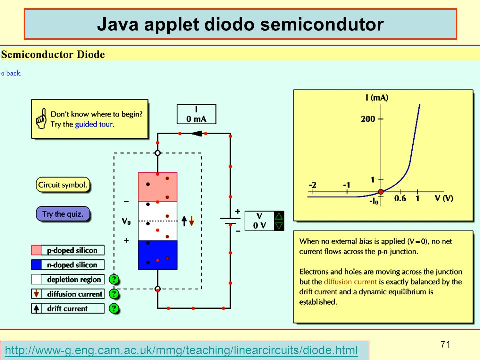
Apresentações semelhantes
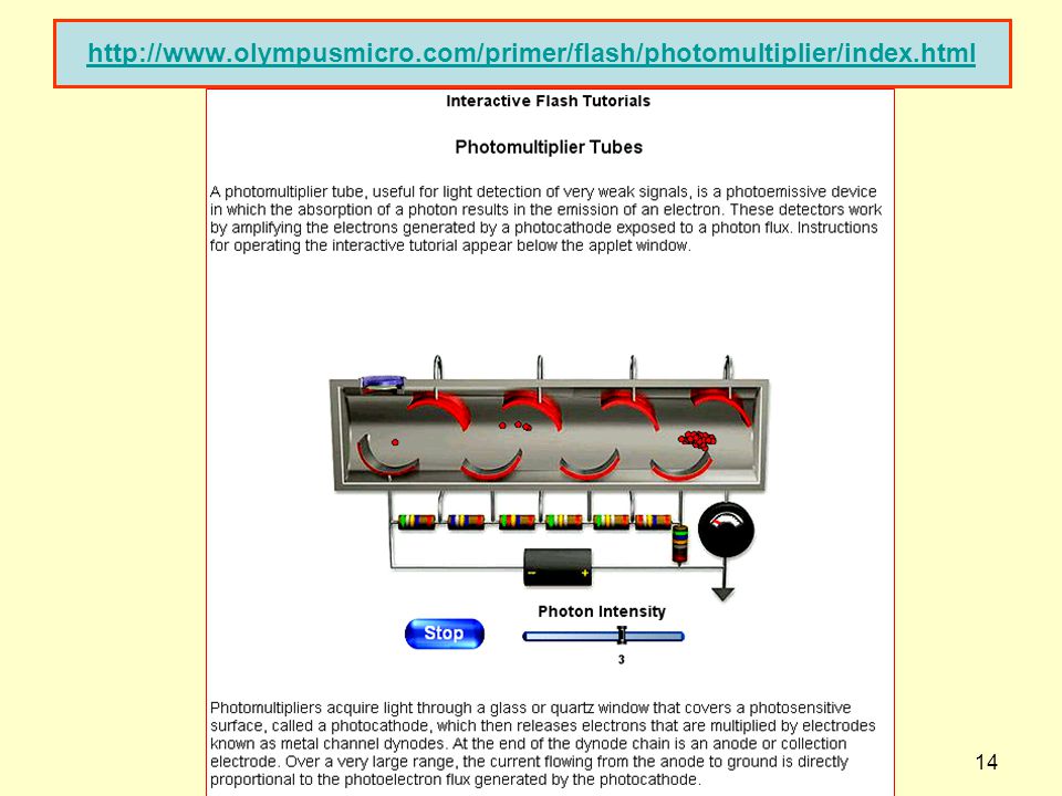
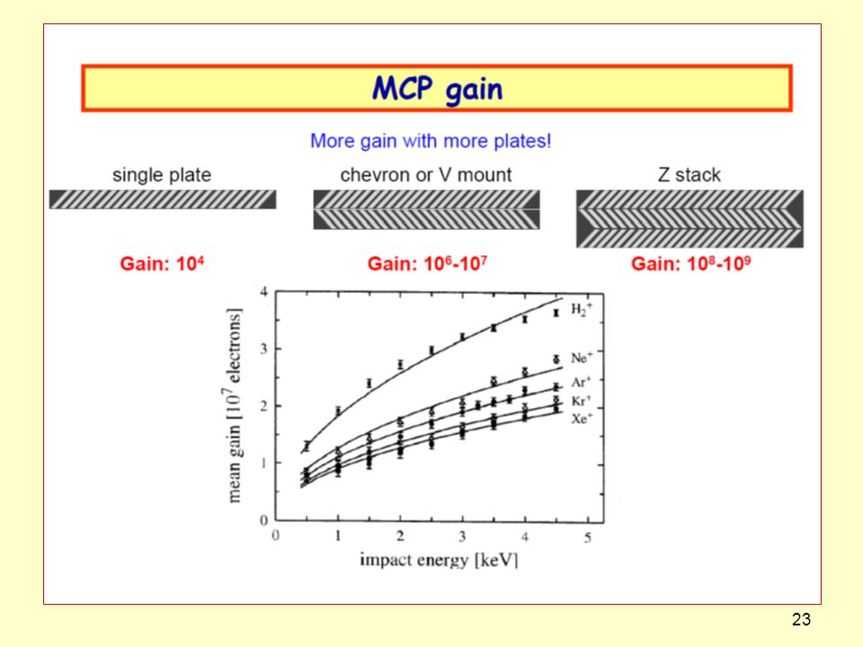
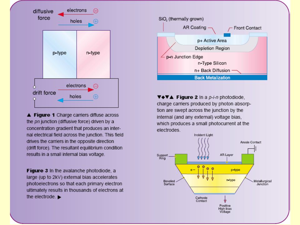

 – Lápides 1, 2, 3» «nomes gravados, 21 de Agosto de 2008» «Ultramar.TerraWeb»>")


. Nenhuns direitos reservados, excepto para fins comerciais. Por favor, não coloque.>")


 2.Comparação.>")

>")


