Carregar apresentação
A apresentação está carregando. Por favor, espere

1
Uma Reflexão Sobre as Tendências da Eletrônica Mauricio Massazumi Oka
LSI/PSI/USP

2
microprocessador (PC) notebooks servidores e roteadores (Internet)
"Technology Drivers" memória (PC) microprocessador (PC) notebooks servidores e roteadores (Internet) serviço móvel
 microprocessador (PC) notebooks. servidores e roteadores (Internet) serviço móvel.")
3
Sistema Eletrônico em Níveis Hierárquicos
de Subsistemas Lâmina Nível 0 Nível 1 Nível 2 Nível 3 Nível 4

4
1) Placas de CI (PWB) 2) Indústria de Semicondutores 3) Encapsulamento 4) Convergência: PCI e encapsulamento
 Encapsulamento. 4) Convergência: PCI e encapsulamento.")
5
A Placa de Circuito Impresso (PCI)
baixo valor agregado reduzir defeitos por número de solda

6
PCB Market 1999 $35 Billion 2002 $38 Billion Multilayer
U.S. (28%), Japan (27%) Taiwan (8-9%), Rest of World
, Japan (27%) Taiwan (8-9%), Rest of World.")
7
Through hole

8
SMT (Surface Mount Technology)
Dupla face Multi camadas Maior densidade ZL = jwL meado dos anos 60 - Ind. Aero-espacial

9
Through Hole vs. SMT

18
Região 1: Pré-Aquecimento
Região 2: Ativação Região 3: Refusão Região 4: Resfriamento

19
Laminado para Dupla Face

20
Fabricação de Laminado

21
Multicamadas

22
NEMA: National Electrical Manufacturers Association

23
Malha de Fibra de Vidro

24
Folha de Cobre

25
Sistema de Resina Epoxy
epoxide group

26
Promoting the First Application in the World
Business for Lead-free Products ahead of the World 1998 1999 2000 2001 2002 Flow soldering process Lead-free soldering materials World’s first complete elimination of use of lead solder Sn-Cu Video deck Vacuum cleaner World’s first lead-free product by flow process 227 ℃ TV Sn-Ag-Cu Reflow soldering process 220 ℃ Car audio system Portable Personal cassette player Expand to all products Sn-Ag-Bi-In MD player 210~205 ℃ DVC Sn-Zn-Bi Current solder: Sn-Pb World’s first lead-free product by reflow process 197 ℃ Melting point: 183 ℃ Notebook PC Number of products adopting lead-free solder 1 2 16 (6,000,000 sets in total) 188
 188.")
27
Advanced Packaging June 2004

28
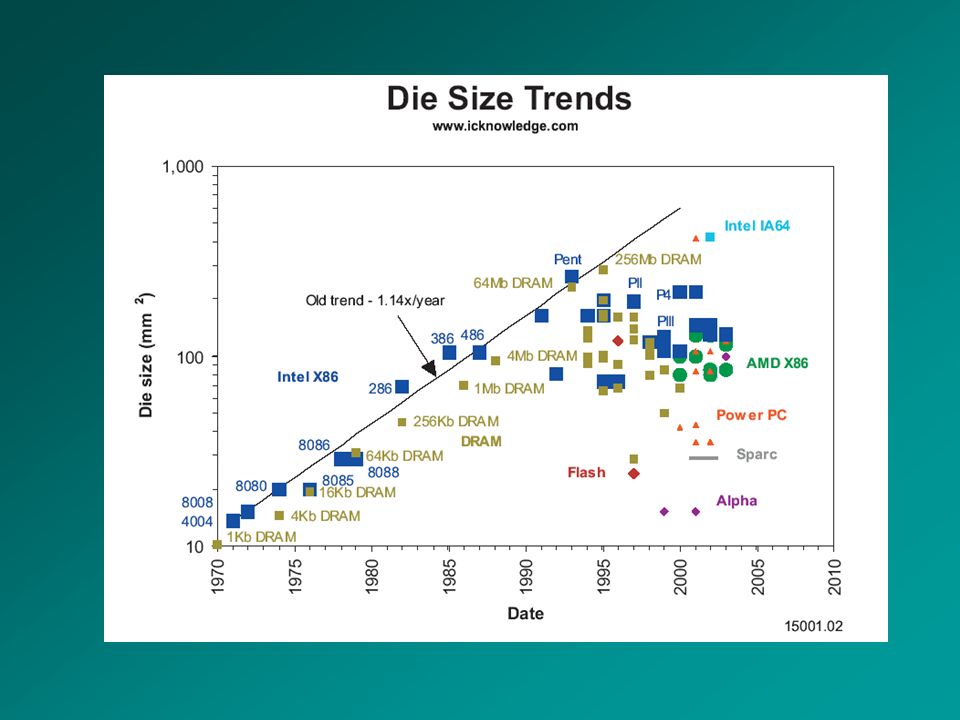
Dimensão Mínima Feature dimension, mmx10-3 Year 1960 1970 1980 1990
Semiconductor Industry PWB Industry 1960 1970 1980 1990 0.25 2.5 25 250 (1270) Feature dimension, mmx10-3 Year
 Feature dimension, mmx10-3. Year.")
29
Indústria de Semicondutores
altíssimo valor agregado 1) reduzir número de pontos de solda 2) processo em lote e escalamento
 reduzir número de pontos de solda. 2) processo em lote e escalamento.")
30
Mercado de Semicondutores
2000: $204,4B 2001: $139,0B

31
Custo de Processamento 2N706 (Transistor mesa - Fairchild) Minuteman
ENIAC: válvulas, 140 kW 2N706 (Transistor mesa - Fairchild) Minuteman amostra: US$ 250 volume: US$ 100 custo: US$ 0,50
 Minuteman. amostra: US$ 250. volume: US$ 100. custo: US$ 0,50.")
32
Custo de Processamento

33
Lei de Moore (1965) Electronic Magazine
 Electronic Magazine")
34
Lei de Escalamento - Dennard (IBM) 1973
CMOS Lei de Escalamento - Dennard (IBM) 1973
")
35
Itanium 2 (0,18 um, 19,5 x 21,6 mm, 421 mm2, 221M Tr, 1 GHz, 130W)
Processador Processo Vertical Horizontal Área Willamette 180 nm 15,7 mm 13,8 mm 217 mm2 Northwood 130 nm 11,27 mm 127 mm2 Itanium 2 (0,18 um, 19,5 x 21,6 mm, 421 mm2, 221M Tr, 1 GHz, 130W)
")
36
Pentium 4: FC-PBGA 2 de 478 pinos

37
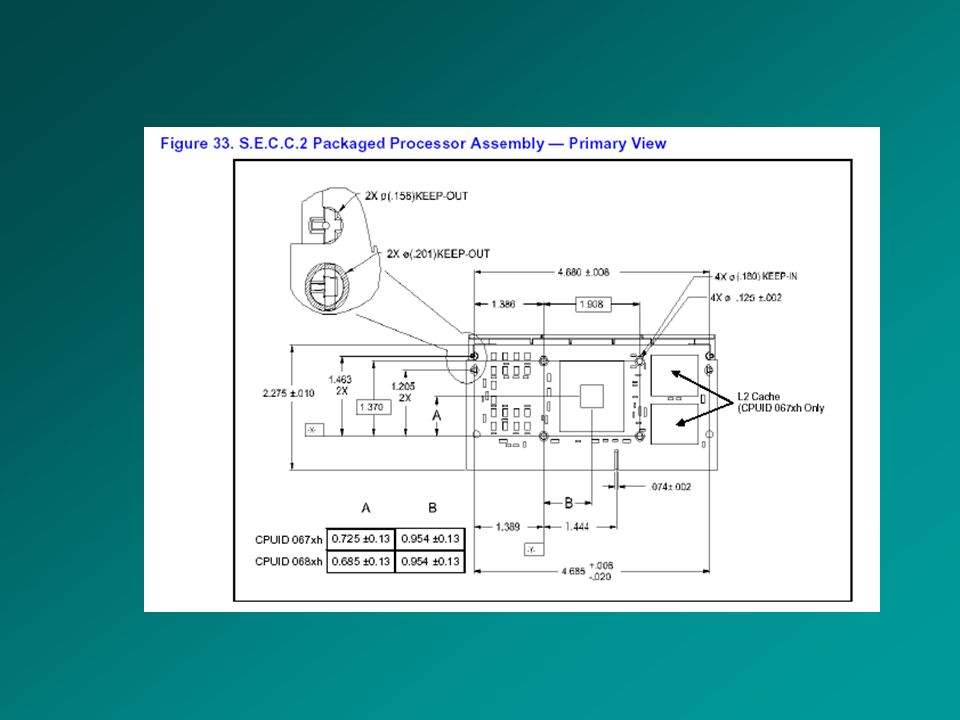
Pentium II e III de 242 contatos
S.E.C.C.2 : Single Edge Contact Cartridge 2

40
Itanium 2 16KB+16KB L1 cache (dados e instruções), 256KB L2
19,5 x 21,6 mm, 421 mm2, 221M Tr, 1 GHz, 130W 16KB+16KB L1 cache (dados e instruções), 256KB L2 1,5MB L3 cache: 221M Tr 6,0MB L3 cache (Madison ): ~ 500M Tr
, 256KB L2. 1,5MB L3 cache: 221M Tr. 6,0MB L3 cache (Madison ): ~ 500M Tr.")
41
NVIDIA GeForce 6800 Ultra (NV 40)
Consumo do GPU: estimado 120W máximo Mais de 220 M de transistors Tecnologia de 0,13 m Die size: 305 mm2 BGA flip-chip de 40mm x 40mm Pin count: 1309 Clock do core: 400 MHz

43
Copper with SiOF Low K ILD
ULSI Process Roadmap 0.50 3.3 volts 0.35 2.5 volts 0.27 0.18 1.8 volts 0.15 1994 1995 1996 1997 1998 0.13 1.5 volts 1999 Process Performance 2000 2001 0.10 1.2 volts 120 MHz 200 MHz 300 MHz 350 MHz 400 MHz 600 MHz 1000 MHz Dual Inlaid Copper Interconnect TFSOI Buried Oxide Silicon Substrate Copper with SiOF Low K ILD Production Dates

44
O encapsulamento de CIs
(plásticos) proteção do CI teste retrabalho
 proteção do CI. teste. retrabalho.")
45
Total 2003: US$ 6,5 B

46
Encapsulamento de CIs

47
DIP (Dual Inline Package)
pitch: 2,54 mm / 64 pinos

48
QFP (Quad Flat Pack) & Fine Pitch
 & Fine Pitch")
49
QFP vs. BGA

50
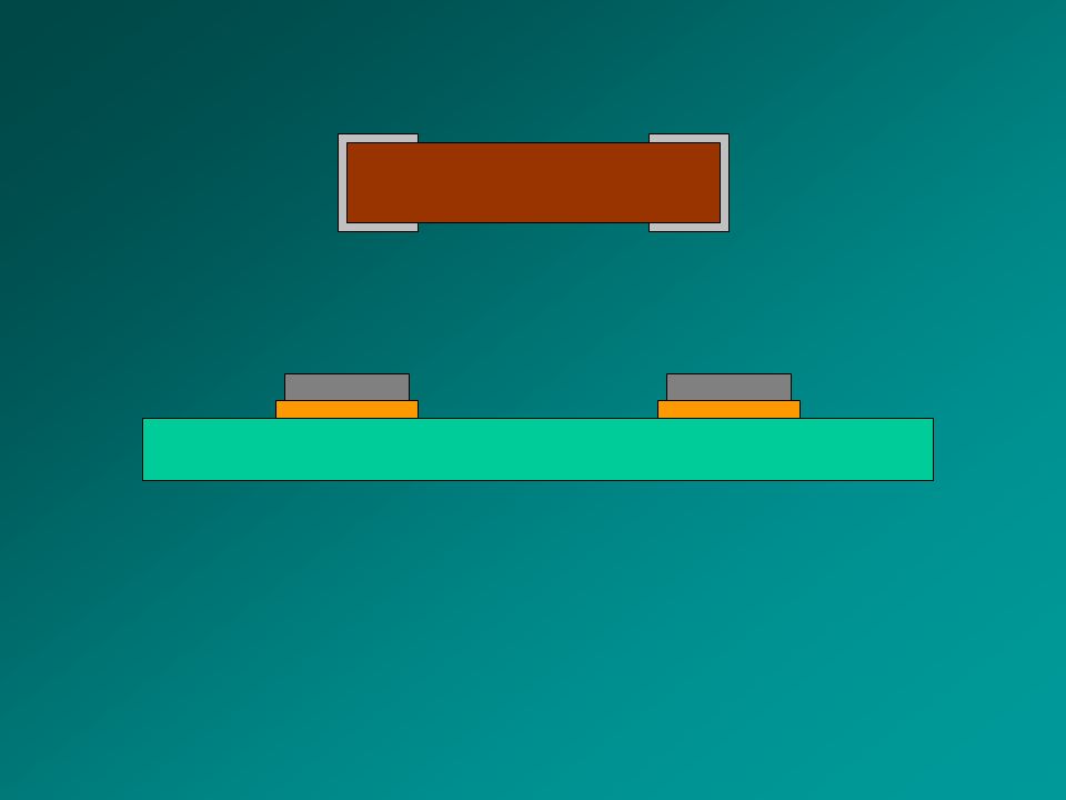
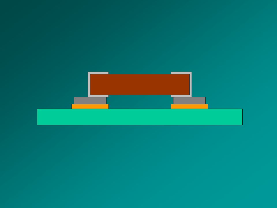
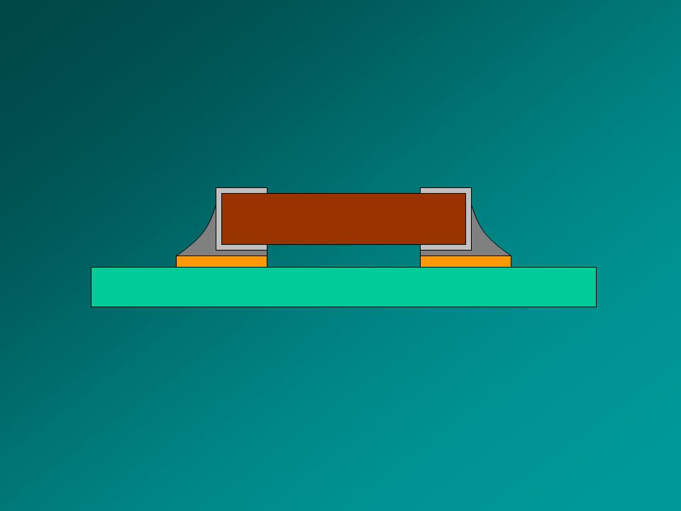
C4: Controlled Collapse Chip Connection IBM (1969)
BGA (Ball Grid Array) C4: Controlled Collapse Chip Connection IBM (1969) epóxi BT (substrato) vias térmicas vias sinal/terra máscara de solda resina BT (Bismaleimide Triazine)
 C4: Controlled Collapse. Chip Connection. IBM (1969) epóxi BT (substrato) vias térmicas. vias sinal/terra. máscara de solda. resina BT (Bismaleimide Triazine)")
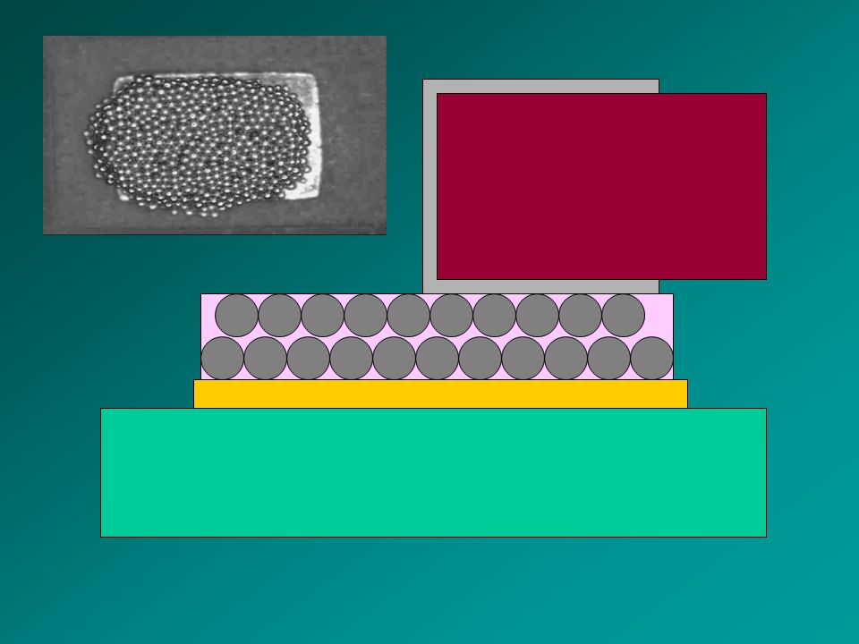
51
BGA (Ball Grid Array)
")
53
JEDEC J-STD-020. classification for moisture-sensitive components · Level 1 — unlimited floor life at 30°C/85% RH · Level 2 — one year floor life at 30°C/60% RH · Level 2a — four week floor life at 30°C/60% RH · Level 3 — 168 hour floor life at 30°C/60% RH · Level 4 — 72 hour floor life at 30°C/60% RH · Level 5 — 48 hour floor life at 30°C/60% RH · Level 5a — 24 hour floor life at 30°C/60% RH · Level 6 — time on label floor life at 30°C/60% RH

54
IPC/JEDEC J-STD-033 Package thickness less than or equal to 1.4 mm: For levels 2a through 5a, bake time ranges from 4 to 14 hours at 125°C, or 5 to 19 days at 40°C. Package thickness less than or equal to 2.0 mm: For levels 2a through 5a, bake time ranges from 18 to 48 hours at 125°C, or 21 to 68 days at 40°C. Package thickness less than or equal to 4.0 mm: For levels 2a through 5a, bake time is 48 hours at 125°C, or 67 or 68 days at 40°C.

55
Convergência: PCI e encapsulamento

56
Type Area Weight QFP 100% 100% BGA ~50% ~50% TAB ~40% ~40%
30 mm Type Area Weight QFP 100% 100% BGA ~50% ~50% TAB ~40% ~40% COB ~25% ~10% CSP ~25% ~10% Flip chip ~10% ~5% Type Area Weight QFP 100% 100% BGA ~50% ~50% TAB ~40% ~40% COB ~25% ~10% CSP ~25% ~10% Flip chip ~10% ~5% 20 mm 15 mm 10 mm (0.4 in.) JSH Trend 9
 JSH. Trend 9.")
57
DCA (Direct Chip Attachment)
TAB: Tape Automated Bonding Filme de polímero com padrões de metal (Cu eletrodepositado)
")
58
DCA (Direct Chip Attachment)
Wire Bonding Flip chip

59
CET & KGD

60
Efeito do Underfill

61
UBM: Under Bump Metalization

62
Tendências do DCA

63
CSP (Chip Scale Package) HDI (High Density Interconnect)
 HDI (High Density Interconnect)")
64
Interposer

65
CSP (Chip Scale Package)
")
66
MCM (Multi Chip Module)
")
67
Coombs

68
HDI (High Density Interconnect)
PTFE: politetrafluoroetileno Teflon

69
HDI (High Density Interconnect)
fibras aramida: Kevlar

70
HDI (High Density Interconnect)
")
71
Tessera: Folded Stacked Technology

72
3D - µZ™ Chip Stack package utiliza tecnologia µBGA® da Tessera

73
SOP: 35 x 35 mm em painéis de 600 x 600 mm
SOC / MCM / SiP / SOP SOP: 35 x 35 mm em painéis de 600 x 600 mm atual: 50 componentes/cm2 / futro: 10k componentes/cm2

74
SOP

75
warpage aceitável

77
Material para isolação

78
Conclusões

79
Tendência: Sistema Eletrônico
Portabilidade (Menor, Low Power, Wireless) Maior Funcionalidade Novas Funções Ubíquo
 Maior Funcionalidade. Novas Funções. Ubíquo.")
80
SOC (Analógico + Digital)
Tendência da Microeletrônica Escalamento SOC (Analógico + Digital) Sensores e Atuadores Design Center IP Fab-less
 Sensores e Atuadores. Design Center. IP. Fab-less.")
81
Dimensões Críticas ~10 um
Tendência do Encapsulamento e PWB Convergência? Dimensões Críticas ~10 um Novos Materias Novos Processos Mais do que proteção Co-design

Apresentações semelhantes


 – Lápides 1, 2, 3» «nomes gravados, 21 de Agosto de 2008» «Ultramar.TerraWeb»>")
 – Universidade Federal de Campina Grande (UFCG)EELA Grid School – December 04, 2006 Enhancing SegHidro/BRAMS.>")


>")


. Nenhuns direitos reservados, excepto para fins comerciais. Por favor, não coloque.>")


